Semiconductor device and method of forming the same

A technology for semiconductors and devices, applied in the field of semiconductor devices and their formation, can solve problems such as affecting the performance of semiconductor devices, short-circuiting of contact structures, etc., and achieve the effects of improving the etching selection ratio, reducing the ratio, and avoiding short-circuit problems.

Active Publication Date: 2020-03-10
SEMICON MFG INT (SHANGHAI) CORP +1
View PDF3 Cites 0 Cited by
  • Summary
  • Abstract
  • Description
  • Claims
  • Application Information

AI Technical Summary

Problems solved by technology

[0004] However, when using self-aligned contact technology to form a contact structure on the source or drain, the contact structure is easily in contact with the gate and short circuit occurs, which affects the performance of semiconductor devices

Method used


Image

  • Semiconductor device and method of forming the same
  • Semiconductor device and method of forming the same
  • Semiconductor device and method of forming the same

Examples


Embodiment Construction

[0034] Embodiments of the present invention provide a semiconductor device and a method for forming the same, which will be described in detail below with reference to the accompanying drawings.

[0035] Figure 1 to Figure 7 is a schematic cross-sectional structure diagram of the intermediate structure of the method for forming a semiconductor device according to the first embodiment of the present invention.

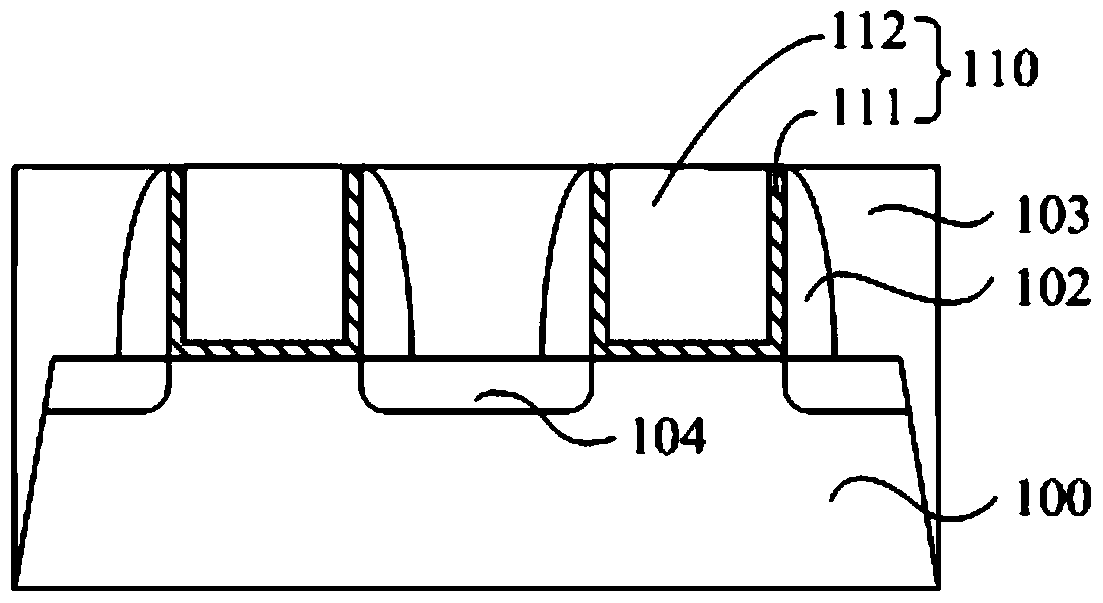
[0036] refer to figure 1 , providing a substrate 100, the surface of the substrate 100 is formed with a gate structure 110, a first dielectric layer 103, and spacers 102 on both sides of the gate structure 110, wherein the gate structure 110 and the spacers 102 are located on the In the first dielectric layer 103, and the top surfaces of the gate structure 110 and the spacer 102 are flush with the top surface of the first dielectric layer 103, the first dielectric layer 103 has the same structure as the sidewall 102 On adjacent side surfaces, source / drain regions 104...


PUM

PropertyMeasurementUnit
sizeaaaaaaaaaa
sizeaaaaaaaaaa
thicknessaaaaaaaaaa

Abstract

The invention provides a semiconductor device and a formation method thereof. The formation method includes providing a substrate, wherein a gate structure, a first dielectric layer and side walls disposed on two sides of the gate structure are formed on the surface of the substrate and the first dielectric layer has side faces adjacent to the side walls; removing a part of the side walls and exposing a part of the side faces of the first dielectric layer; removing the first dielectric layer from the top surface of the first dielectric layer and the exposed side faces of the first dielectric layer, removing a part of the gate structure and forming a first opening in the remained first dielectric layer; forming a coverage layer filling the first opening and flush with the top surface of the remained first dielectric layer, wherein the side wall of the coverage layer has a protrusion disposed on the remained first dielectric layer. According to the invention, the protrusion realizes a shielding and protection effect on the side walls, so that the proportion of an etched part of the side walls is reduced, the isolation between a contact structure and the gate structure is enhanced and a short circuit problem is avoided.

Description

technical field [0001] The invention relates to the technical field of semiconductor manufacturing, in particular to a semiconductor device and a forming method thereof. Background technique [0002] In the prior art method for forming a semiconductor device, the electrical connection between multilayer circuits on a silicon wafer is realized through a contact structure. When forming the contact structure, first, the interlayer dielectric layer (ILD) is photoetched to form a trench or a through hole; then, conductive material is filled in the trench or the through hole to form the contact structure. With the rapid development of ultra-large-scale integrated circuits, the feature size of components is continuously reduced, which puts forward higher requirements for photolithography. [0003] In a semiconductor manufacturing process, a self-aligned contact (Self Alignment Contact, SAC) technology is usually used to form a contact (Contact) structure. The self-aligned contact...

Claims


Application Information

Patent Timeline
Patent Type & Authority Patents(China)
IPC IPC(8): H01L27/04H01L21/82
CPCH01L21/82H01L27/04
Inventor 张城龙袁光杰张海洋
Owner SEMICON MFG INT (SHANGHAI) CORP
Why Eureka
Try Eureka