Fast ferroelectric transistor memory based on two-dimensional organic molecular semiconductors and preparation thereof

A technology of ferroelectric transistors and organic molecules, which is applied in semiconductor/solid-state device manufacturing, semiconductor devices, electric solid-state devices, etc., can solve the problems of no advantages and hinder the state transition speed of organic memory, and achieve the effect of improving the operation speed

Inactive Publication Date: 2017-10-20
NANJING UNIV
View PDF2 Cites 7 Cited by
  • Summary
  • Abstract
  • Description
  • Claims
  • Application Information

AI Technical Summary

Problems solved by technology

In some previous research work, the two state transitions of ferroelectric organic field effect transistor memory are generally tens to hundreds of milliseconds, but this is obviously no advantage com

Method used


Image

  • Fast ferroelectric transistor memory based on two-dimensional organic molecular semiconductors and preparation thereof
  • Fast ferroelectric transistor memory based on two-dimensional organic molecular semiconductors and preparation thereof
  • Fast ferroelectric transistor memory based on two-dimensional organic molecular semiconductors and preparation thereof

Examples


Embodiment Construction

[0029] The preferred embodiments of the present invention will be described in detail below in conjunction with the accompanying drawings, so that the advantages and features of the present invention can be more easily understood by those skilled in the art, so as to define the protection scope of the present invention more clearly.

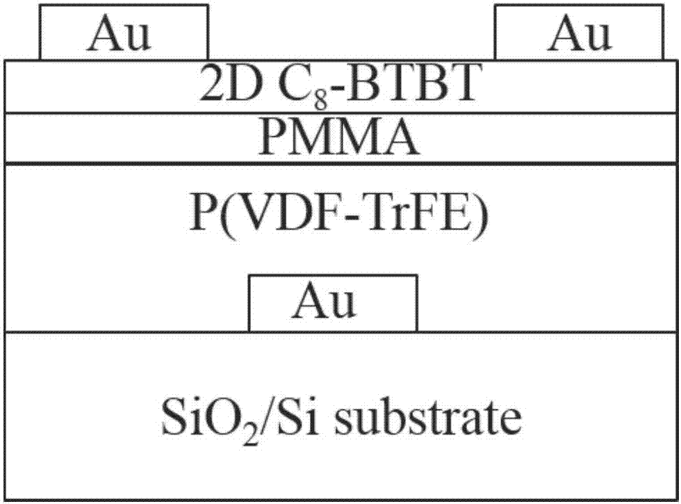
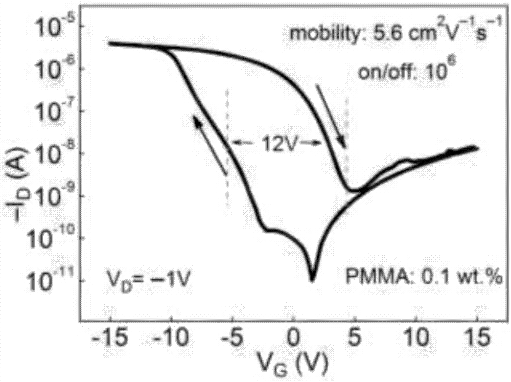
[0030] see figure 1 , an embodiment of the present invention: a preparation of a fast ferroelectric transistor memory based on a two-dimensional organic molecular semiconductor, comprising:

[0031] Two-dimensional organic molecular semiconductor ferroelectric transistor memory is an important application of two-dimensional organic materials in memory. Compared with inorganic memory, the main solution is: large storage density, small size devices, simple Thin film preparation process, large area preparation; compared with some other organic memories, the semiconductor layer is thinner, the carrier mobility of the device is greater, and the data s...


PUM

PropertyMeasurementUnit
Thicknessaaaaaaaaaa
Lengthaaaaaaaaaa
Widthaaaaaaaaaa

Abstract

A fast ferroelectric transistor memory based on two-dimensional organic molecule semiconductors is prepared in a way that heavily doped p-type silicon is taken as a substrate and 50-250 nm silicon dioxide is grown and used as an insulating layer; a layer of 20-50 nm gold is prepared on the silicon dioxide by thermal evaporation and used as the gate, and then a layer of ferroelectric polymer material, poly (vinylidene fluoride-trifluoroethylene), is spin-coated on the gate; and a layer of untrathin polymethyl methacrylate (PMMA) with thickness of 2-10 nm and a dioctyl benzothiophene benzothiophene semiconductor layer (C8-BTBT) with thickness of 5-10 nm are grown respectively on P (VDF-TrFE) by the floating coffee effect and the phase separation method, wherein the passivation layer PMMA is under the two-dimensional semiconductor layer C8-BTBT, gold is deposited on the semiconductor layer as a source and a drain to prepare a two-dimensional organic molecular semiconductor ferroelectric transistor memory having a bottom gate top contact structure.

Description

technical field [0001] The invention relates to the fields of two-dimensional molecular crystal, ferroelectric polymer, semiconductor technology, organic transistor memory and the like, in particular to a fast organic memory and its preparation. Background technique [0002] With the rapid development of electronic information technology, memory, as a memory device used to store information in modern information technology, has become an indispensable element of various electronic information products, such as computers, smart phones, MP3, etc. At present, silicon-based electrical memory based on traditional semiconductors has the advantages of fast storage and long storage time, and is still a hot spot in the application of modern memory, and this traditional memory mainly uses the changes of magnetic signals, electrical signals, and optical signals of materials to Realize information storage. However, the traditional memory also has problems such as large size, complicate...

Claims


Application Information

Patent Timeline
IPC IPC(8): H01L51/05H01L51/30H01L51/40
CPCH10K71/12H10K85/6576H10K10/471H10K10/466
Inventor 李昀宋磊王宇施毅
Owner NANJING UNIV
Why Eureka
Try Eureka