Waveguide structure and preparation method

A technology of waveguide structure and waveguide, which is applied in the direction of optical waveguide light guide, coupling of optical waveguide, light guide, etc., can solve the problems of matching, limited beam expansion effect of light spot, and high processing technology requirements of cone tip structure

Active Publication Date: 2020-01-10
HUAWEI TECH CO LTD
View PDF5 Cites 0 Cited by
  • Summary
  • Abstract
  • Description
  • Claims
  • Application Information

AI Technical Summary

Problems solved by technology

At present, the main solutions for silicon optical coupling are: one coupling solution is grating coupler (grating coupler) vertical coupling, which has the characteristics of mode field matching, but the loss of grating coupler itself is relatively large, and it is sensitive to polarization and wavelength, making The use of this coupling scheme is limited; another coupling scheme is end-face coupling, which uses a tapered waveguide to achieve spot beam expansion. Fiber Mode Spot Size Matching

Method used


Image

  • Waveguide structure and preparation method
  • Waveguide structure and preparation method
  • Waveguide structure and preparation method

Examples


Embodiment Construction

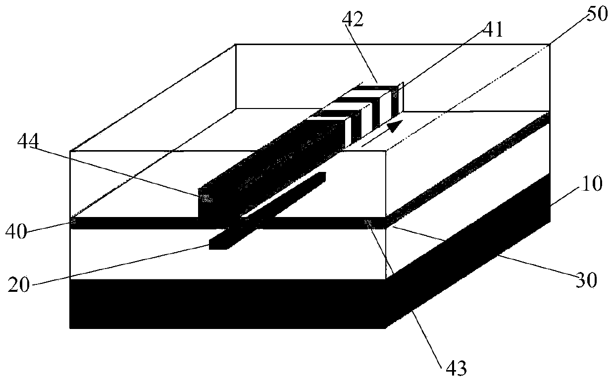
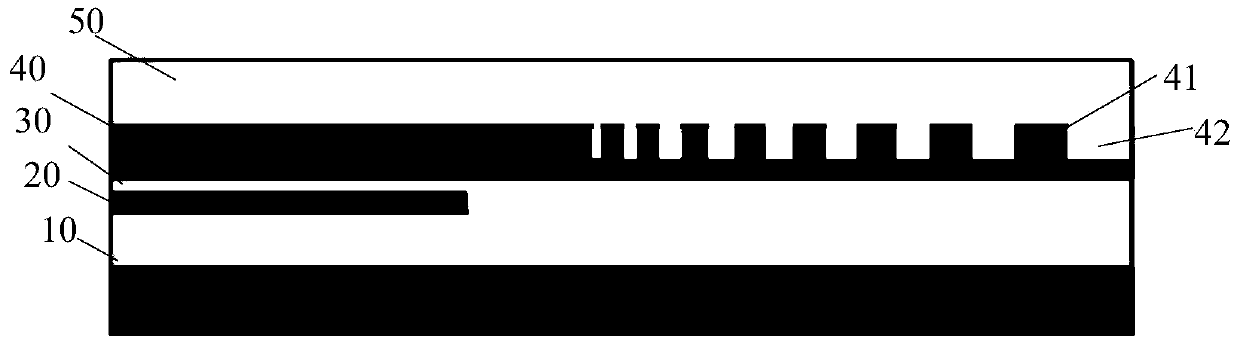
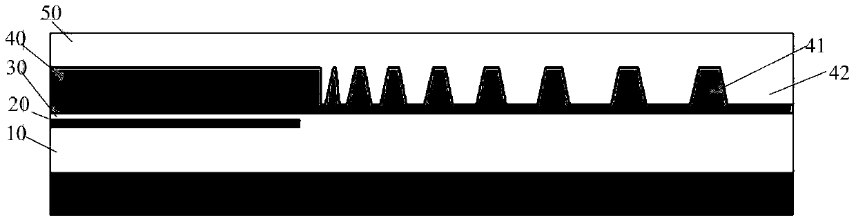
[0033] In order to make the purpose, technical solutions and advantages of the embodiments of the present invention more clear, the technical solutions of the embodiments of the present invention will be clearly and completely described below in conjunction with the drawings of the embodiments of the present invention. Apparently, the described embodiments are only some of the embodiments of the present invention, not all of them. Based on the embodiments of the present invention, all other embodiments obtained by persons of ordinary skill in the art without making creative efforts shall fall within the protection scope of the present invention.

[0034] Unless otherwise defined, technical terms or scientific terms used herein shall have the usual meanings understood by those having ordinary skill in the art to which the present invention belongs. "First", "second", "third" and "fourth" and the like used in the present invention are used to distinguish different objects, not t...


PUM

PropertyMeasurementUnit
thicknessaaaaaaaaaa
thicknessaaaaaaaaaa
refractive indexaaaaaaaaaa

Abstract

A waveguide structure is provided. A silicon substrate layer, a silicon waveguide layer, a first silicon dioxide layer, a silicide waveguide layer, and a second silicon dioxide layer are stacked in sequence, the silicon waveguide layer is a conical waveguide layer, the silicon waveguide layer and the silicide waveguide layer are coupled by using an evanescent wave, the silicide waveguide layer includes multiple first waveguide blocks and multiple second waveguide blocks, a material of the first waveguide blocks is the same as a material of the silicide waveguide layer, and a refractive index of a material of the second waveguide blocks is lower than a refractive index of the material of the first waveguide blocks. By using the waveguide structure, a waveguide flare size can be increased, so as to match a mode size of a fiber core of an optical fiber.

Description

technical field [0001] The invention relates to the field of optical communication devices, in particular to a waveguide structure and a preparation method. Background technique [0002] With the upgrading of network products, the size and power consumption of modules used in the network are constantly decreasing to meet the needs of continuous cost reduction and performance improvement. Due to its unique characteristics such as low cost, ultra-small size, and low power consumption, silicon-based photonic devices have attracted extensive attention from the industry in recent years, and have become one of the key considerations in the upgrading of network products. [0003] In the prior art, since the spot size (0.3um) of the silicon optical waveguide is much smaller than the mode spot size (9um) of the fiber core, the coupling loss will be large due to the mismatch of the optical coupling mode field size between the two. At present, the main solutions for silicon optical co...

Claims


Application Information

Patent Timeline
Patent Type & Authority Patents(China)
IPC IPC(8): G02B6/122G02B6/12G02B6/136G02B6/26
CPCG02B6/12G02B6/122G02B6/1228G02B6/136G02B6/26G02B2006/12038G02B6/124G02B6/02085G02B6/12002G02B6/12007G02B2006/12061
Inventor 周立兵李唯实
Owner HUAWEI TECH CO LTD
Why Eureka
Try Eureka