A fast turn-off silicon-on-insulator lateral insulated gate bipolar transistor device

A bipolar transistor, silicon-on-insulator technology, applied in semiconductor devices, electrical components, circuits, etc., can solve the problems of not being greatly improved, small chip area, unstable device performance, etc., and achieve enhanced conductivity. Modulation effect, reduction of drift region resistance, effect of equalization of carrier distribution

Active Publication Date: 2020-03-24
SOUTHEAST UNIV +1
View PDF4 Cites 0 Cited by
  • Summary
  • Abstract
  • Description
  • Claims
  • Application Information

AI Technical Summary

Problems solved by technology

In order to reduce the conduction voltage drop of the device, a planar gate SOI-LIGBT structure with a U-shaped channel has recently been proposed. By adopting this structure, the planar gate SOI-LIGBT device with a U-shaped channel achieves a lower conduction voltage drop. , however, in these SOI-LIGBT structures, due to the existence of the JFET region, the on-resistance is increased, and the on-voltage drop cannot be effectively reduced. Therefore, a vertical trench structure device is proposed on this basis, and this structure eliminates The JFET area is reduced, and the conduction voltage drop is reduced, but the effect is not very good, and the voltage drop in the drift region where the on-resistance is larger has not been greatly improved; and in order to obtain a lower conduction voltage drop , it will increase the number of carriers stored in the drift region. During the turn-off process, this part of the carriers will take a long time to remove, which will prolong the turn-off time of the device and eventually lead to a larger The turn-off loss, so for the vertical trench SOI-LIGBT device with the traditional structure, it is often necessary to make a compromise between the turn-on voltage drop and the turn-off loss
In addition, the large switching power consumption of SOI-LIGBT devices is the bottleneck that restricts monolithic integrated power chips to work at higher frequency, better work energy efficiency, and smaller chip area
Therefore, in order to reduce the switching power consumption of the device, some devices with improved structures have been proposed, such as SA-LIGBT and some devices that have undergone electron radiation. These structures can effectively shorten the turn-off time and reduce the turn-off loss, but at the same time It brings new problems, such as the former will have voltage hysteresis during forward conduction, which will reduce the reliability of the device, while the latter may have a large leakage current at high temperature, resulting in unstable device performance

Method used


Image

  • A fast turn-off silicon-on-insulator lateral insulated gate bipolar transistor device
  • A fast turn-off silicon-on-insulator lateral insulated gate bipolar transistor device
  • A fast turn-off silicon-on-insulator lateral insulated gate bipolar transistor device

Examples


Embodiment Construction

[0028] Combine below figure 2 , image 3 , Figure 4 , the present invention is described in detail:

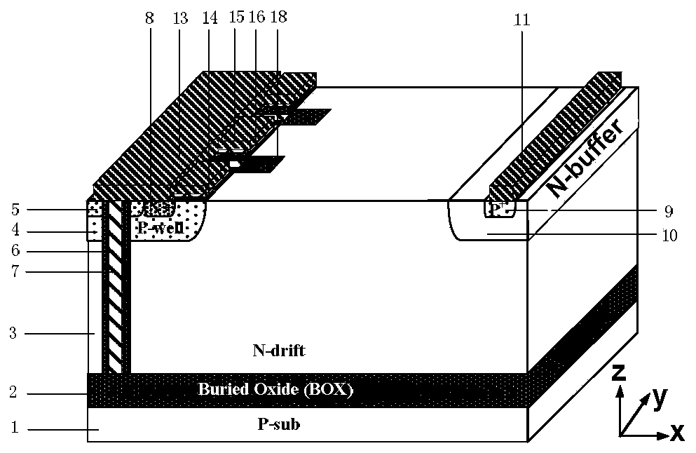
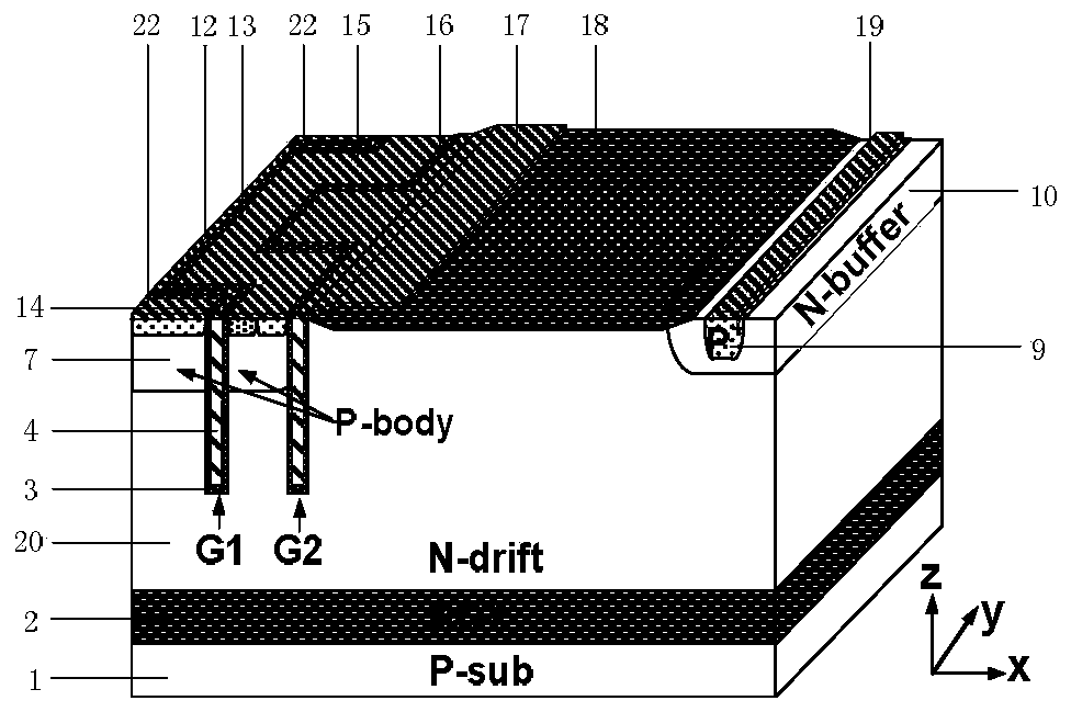
[0029]A fast turn-off silicon-on-insulator lateral insulated gate bipolar transistor device, comprising: a P-type substrate 1, a buried oxygen 2 is arranged on the P-type substrate 1, and an N-type drift region 20 is arranged on the buried oxygen 2 , N-type buffer zone 10 and P-type body region 7 are respectively arranged on both sides of N-type drift region 20, and heavily doped P-type collector region 9 is arranged in N-type buffer zone 10, and heavily doped P-type A collector metal 19 is connected to the collector region 9, a heavily doped N-type emitter region 11 is provided in the P-type body region 7, and a heavily doped The doped P-type emitter region 8b is connected with the second emitter metal 15 on the above-mentioned heavily doped P-type emitter region 8b and the heavily doped N-type emitter region 11, and a second emitter metal 15 is arranged above the N-type...


PUM


Abstract

A fast turn-off silicon-on-insulator lateral insulated gate bipolar transistor, with buried oxygen on a P-type substrate, an N-type drift region on the buried oxygen, an N-type buffer zone and a P-type body on it In the N-type buffer area, there is a P-type collector area, which is connected to the collector metal, and an N-type emitter area is set in the P-type body area, and a P-type emitter area is set on the right side of it. The emitter metal is connected to the electrode area, a field oxygen layer is provided above the N-type drift area, and a longitudinal groove is provided on the left side of the N-type emitter area, and a silicon dioxide or other pressure-resistant medium is arranged inside. The polysilicon layer is connected with a gate metal, and a P-type emitter block is provided on the left side of the vertical groove, and an emitter metal is connected thereon, and a vertical groove is arranged between the field oxygen layer and the P-type emitter region. A groove, in which a polysilicon layer wrapped by silicon dioxide or other pressure-resistant medium is provided, on which a gate metal is connected, and an oxide layer is provided between the gate metal and the emitter metal.

Description

technical field [0001] The invention mainly relates to the technical field of power semiconductor devices, and is a novel fast-turn-off silicon-on-insulator lateral insulated gate bipolar transistor, which is especially suitable for realizing accurate control of motor systems in monolithic integrated power chips. Background technique [0002] Insulated gate bipolar transistor IGBT is a composite device of MOSFET and bipolar transistor, and has the characteristics of both MOSFET and bipolar transistor. It not only has the characteristics of easy driving of MOSFET, but also has the advantages of large voltage and current capacity of power transistor. , with a good tradeoff between on-state current and switching losses. Silicon-on-insulator lateral insulated gate bipolar transistor (SOI-Lateral Insulated Gate Bipolar Transistor, SOI-LIGBT) is a typical device based on SOI technology, which has the advantages of easy integration, high withstand voltage, strong drive current capa...

Claims


Application Information

Patent Timeline
Patent Type & Authority Patents(China)
IPC IPC(8): H01L29/739H01L29/08H01L29/06
CPCH01L29/0661H01L29/0808H01L29/0821H01L29/7394
Inventor 祝靖汤清溪张龙孙伟锋陆生礼时龙兴
Owner SOUTHEAST UNIV
Why Eureka
Try Eureka