Quantum dot light emitting diode and manufacturing method thereof

A quantum dot light-emitting and diode technology, which is applied in semiconductor/solid-state device manufacturing, electrical components, circuits, etc., can solve the problems of poor device performance, unmodified electron transport layer, unstable dopant, etc., to reduce refraction Efficiency imbalance, improving light extraction efficiency, and reducing the effect of total light reflection

Inactive Publication Date: 2017-10-24
SUZHOU UNIV
View PDF8 Cites 34 Cited by
  • Summary
  • Abstract
  • Description
  • Claims
  • Application Information

AI Technical Summary

Problems solved by technology

However, due to the low light extraction efficiency, the device performance is poor, and the dopants containing alkali metals are unstable.
[0009] In 2016, Shuming Chen et al. (ACS Appl. Mater. Interfaces 2016, 8, 5493-5498) published an article disclosing an inverted QLED device using ZnO nanoparticles. Since the electron transport layer is not modified, light extraction is limited, and the best The device EQE of performance is only 2.72%

Method used


Image

  • Quantum dot light emitting diode and manufacturing method thereof
  • Quantum dot light emitting diode and manufacturing method thereof
  • Quantum dot light emitting diode and manufacturing method thereof

Examples


Embodiment 1

[0055] In one embodiment, the imprint template adopts soft polydimethylsilane (PDMS), and the shape of the nano-concave-convex structure is as follows: Figure 4 As shown, the period is preferably 400nm, the groove depth is 50nm, and the duty ratio is 0.6.

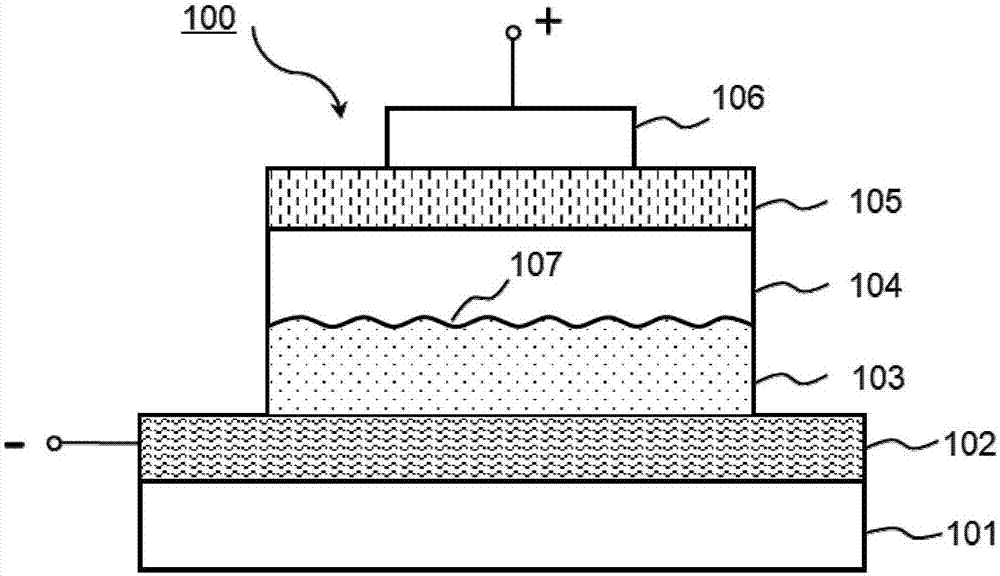
[0056] A quantum dot light-emitting diode with a nano-light extraction structure, including an ITO transparent cathode on a substrate, a ZnO electron transport layer, a CdSe / ZnS quaternary gradient alloy quantum dot light-emitting layer, and a PVK / PEDOT:PSS composite hole transport layer and Al metal anode, the specific manufacturing process of each layer structure is preferably a method such as solution method spin coating, vacuum thermal evaporation, or other known methods. Preferably, in this embodiment, the specific process of device manufacturing is as follows:

[0057] (1) Substrate and cathode cleaning: After the ordinary float glass substrate substrate is cleaned with detergent, a patterned ITO film is sputtered on...

Embodiment 2

[0064] A quantum dot light-emitting diode with an electron transport layer modification layer, including an ITO transparent cathode on a substrate, a ZnO electron transport layer, a PEI modification layer, a CdSe / ZnS quaternary gradient alloy quantum dot light-emitting layer, PVK / PEDOT:PSS Composite hole transport layer and Al metal anode, the specific manufacturing process of each layer structure is preferably solution method spin coating, vacuum thermal evaporation and other methods, or other known methods. Preferably, in this embodiment, the specific process of making quantum dot light-emitting diodes as follows:

[0065] (1) Substrate and cathode cleaning: same as in Embodiment 1.

[0066] (2) Preparation of ZnO precursor solution: same as Example 1.

[0067] (3) Fabrication and modification of the electron transport layer: Spin-coat a layer of ZnO precursor solution on the substrate treated in step (1) in air. The control speed is 4000rpm, the time is 60s, and annealed ...


PUM


Abstract

The invention discloses a quantum dot light emitting diode and a manufacturing method thereof. The quantum dot light emitting diode comprises a substrate, a cathode, an electron transport layer, a quantum dot light emitting layer, a hole transport layer, and an anode stacked in sequence. The quantum dot light emitting diode is characterized in that the upper surface of the electron transport layer is provided with a nano convex-concave structure which is in quasi-periodic or aperiodic shape, and refractive index of the nano convex-concave structure shows gradient changes along an emergent light direction. Efficiency of an inverted structure quantum dot light emitting diode is obviously improved, and the efficiency is far ahead efficiency of other inverted quantum dot devices.

Description

technical field [0001] The invention relates to the technical field of photoelectric devices, in particular to a high-efficiency inverted structure quantum dot light-emitting diode and a preparation method thereof. Background technique [0002] Quantum dot light-emitting diode (QLED) is an electroluminescent device with quantum dots as the light-emitting layer. Quantum dots are semiconductor nanocrystals whose particle size is smaller than or close to the exciton Bohr radius. The three-dimensional scale is usually below 10nm, and the movement of internal electrons and holes in all directions is restricted. Quantum dots used in the field of luminescence generally have a core-shell structure, and the surface is passivated by ligands. Since electrons and holes are quantum confined, quantum dots have discrete energy level structures. This discrete energy level structure makes quantum dots have unique optical properties. Whenever stimulated by light or electricity, the quantum...

Claims


Application Information

Patent Timeline
Patent Type & Authority Applications(China)
IPC IPC(8): H01L51/50H01L51/56
CPCH10K50/115H10K50/16H10K2102/00H10K71/00
Inventor 唐建新许瑞鹏刘悦琪李艳青
Owner SUZHOU UNIV
Why Eureka
Try Eureka