

A deep trench dmos device
A deep groove and device technology, applied in the field of deep groove DMOS devices, can solve the problems of increased junction surface, high production cost, poor body diode reverse recovery characteristics, etc., and achieve the goal of reducing on-resistance and improving reverse withstand voltage performance Effect
- Summary
- Abstract
- Description
- Claims
- Application Information
AI Technical Summary
Problems solved by technology
Method used
Image

Examples
Embodiment 1
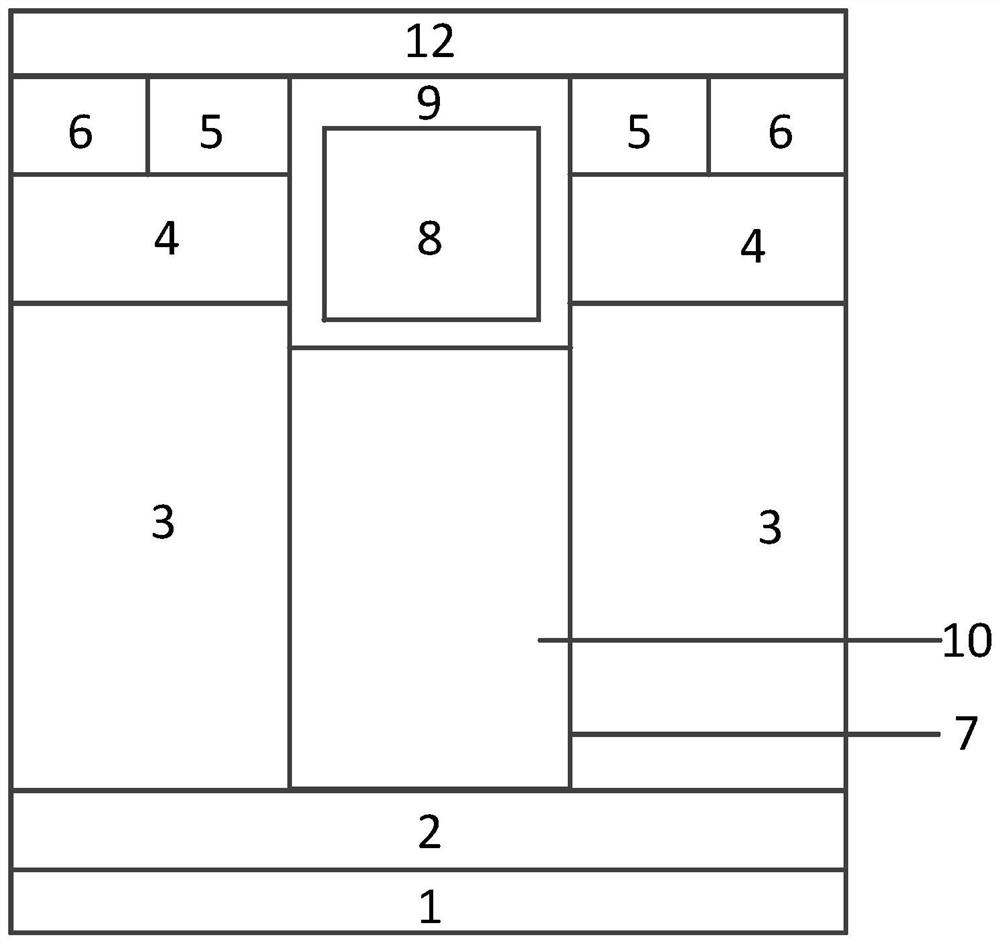
[0026] Such as figure 1 As shown, this embodiment provides a deep trench DMOS device, including: N + Substrate 2, at N + The backside of the substrate 2 is provided with a metallized drain 1, and the N + The front side of the substrate 2 is provided with an N-type drift region 3, and a P-type body region 4 is provided under the surface of the N-type drift region 3, and a deep groove 7 is arranged in the P-type body region 4, and the P-type body regions on both sides of the deep groove 7 4 with N + source region 5 and P + Contact area 6, deep groove 7, N + source region 5 and P + The upper surface of the contact region 6 is in contact with the metallized source 12, the deep groove 7 has a gate electrode 8 and a gate dielectric layer 9, and the junction depth of the upper surface of the gate electrode 8 is less than N + The lower surface junction depth of the source region 5, the lower surface junction depth of the gate electrode 8 is greater than the lower surface junctio...
Embodiment 2
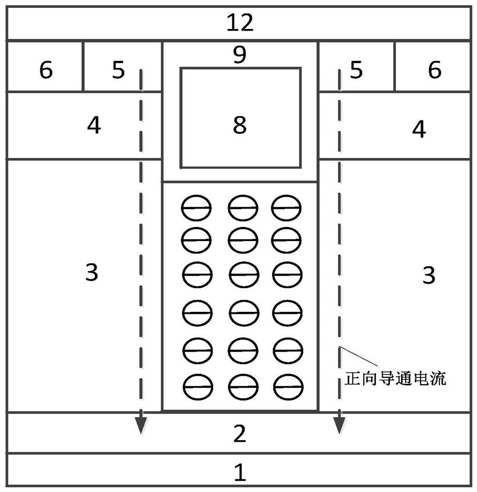
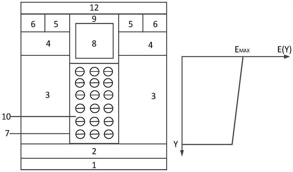
[0039] The structure of this embodiment is the same as that of Embodiment 1 except that the doping amount of negative charges in the strained insulating dielectric region 10 gradually decreases from top to bottom (ie, from the metallized source to the metallized drain).
[0040] This embodiment is an improvement of Embodiment 1. Through the above means, the lateral electric field distribution formed by the N-type drift region 3 and the strained insulating dielectric region 10 can be made more uniform, so that the vertical electric field is closer to the rectangular distribution, and the reverse blocking of the device is further improved. Voltage.
Embodiment 3
[0042] This embodiment provides a deep groove DMOS device, including: P + Substrate 2, at P + The backside of the substrate 2 is provided with a metallized drain 1, on the P + The front side of the substrate 2 is provided with a P-type drift region 3, and a P-type body region 4 is provided under the surface of the P-type drift region 3. There are deep grooves 7 in the P-type body region 4, and the P-type body regions on both sides of the deep groove 7 4 with P + source region 5 and P + Contact zone 6, deep groove 7, P + source region 5 and P + The upper surface of the contact region 6 is in contact with the metallized source 12, the deep groove 7 has a gate electrode 8 and a gate dielectric layer 9, and the junction depth of the upper surface of the gate electrode 8 is less than P + The lower surface junction depth of the source region 5, the lower surface junction depth of the gate electrode 8 is greater than the lower surface junction depth of the N-type body region 4, ...
PUM
 Abstract
Description
Claims
Application Information