TaN thin-film resistor for high-temperature environment and preparation method of TaN thin-film resistor
A high-temperature environment and thin-film resistor technology, which is applied in thin-film resistors, resistor manufacturing, resistors, etc., can solve the problems of decreased adhesion of electrode layers, large TCR changes, and large resistance values, and achieves a small temperature coefficient. , good precision, avoid peeling effect
- Summary
- Abstract
- Description
- Claims
- Application Information
AI Technical Summary
Problems solved by technology
Method used
Image

Examples
preparation example Construction
[0049] A method for preparing a TaN thin film resistor used in a high temperature environment, comprising the following steps:
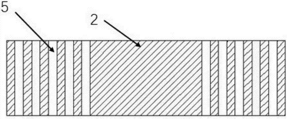
[0050] A) According to the size parameters of the resistance film pattern and electrode pattern to be designed, a photolithographic mask plate corresponding to the resistance pattern and electrode pattern is produced. The area of the resistive film on the resistive pattern mask is designed as a non-transparent area, the grooves, holes and other areas are designed as a light-transmitting area, the electrode area on the electrode pattern mask is designed as a non-transparent area, and the area other than the electrodes is designed as a non-transparent area. The light-transmitting area, so when the resistive pattern mask is used in the exposure process, a non-photosensitive area consistent with the resistive film pattern can be formed on the photoresist, and the photoresist can be formed on the photoresist when the electrode pattern mask is used. Non-...
Embodiment 1
[0057] Example 1: Making a grooved thin film resistor, the size of the resistor is 1.8×0.5×0.25mm 3 , the electrode plane size is 0.5×0.5mm 2 , the effective area of the resistive film is 0.8×0.5mm 2 , including the following steps:
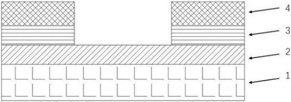
[0058] Step 1: Take a clean, 0.25mm-thick, 3-inch square single-side polished AlN substrate as the substrate 1;
[0059] Step 2, using radio frequency magnetron sputtering technology to deposit a layer of TaN resistance film on the polished surface of the dielectric substrate 1 as the resistance film 2; deposition parameters: the sputtering power is 200W, the nitrogen partial pressure is 3%, and the sputtering pressure is 0.1 Pa, the deposition time is 10min, and the thickness is about 180nm.
[0060] Step 3: Coat a layer of photoresist on the surface of the resistive film 2, spread the glue on the coater at a speed of 2000 rpm for 10 minutes, then use a resistive film mask to expose for 10 seconds under the exposure machine, and develop for...
Embodiment 2
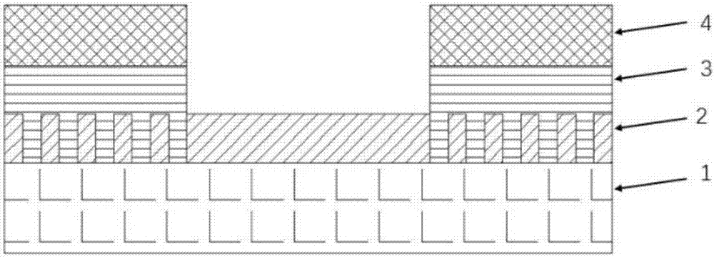
[0069] Example 2: Making a thin film resistor with a cylindrical hole, the size of the resistor is 2.0×0.6×0.25mm 3 , the electrode plane size is 0.6×0.6mm 2 , the effective area of the resistive film is 0.8×0.6mm 2 , including the following steps:
[0070] Step 1: Take a clean 3-inch single-side polished AlN substrate with a thickness of 0.25 mm as the substrate 1;
[0071] Step 2, using radio frequency magnetron sputtering technology to deposit a layer of TaN resistance film on the polished surface of the dielectric substrate 1 as the resistance film 2; deposition parameters: the sputtering power is 200W, the nitrogen partial pressure is 3%, and the sputtering pressure is 0.1 Pa, the deposition time is 10min, and the thickness is about 180nm.
[0072] Step 3: Coat a layer of photoresist on the surface of the resistive film 2, spread the glue on the coater at a speed of 2000 rpm for 10 minutes, then use a resistive film mask to expose for 10 seconds under the exposure ma...
PUM
 Abstract
Description
Claims
Application Information
 - R&D
- Intellectual Property
- Life Sciences
- Materials
- Tech Scout
- Unparalleled Data Quality
- Higher Quality Content
- 60% Fewer Hallucinations
Browse by: Latest US Patents, China's latest patents, Technical Efficacy Thesaurus, Application Domain, Technology Topic, Popular Technical Reports.
© 2025 PatSnap. All rights reserved.Legal|Privacy policy|Modern Slavery Act Transparency Statement|Sitemap|About US| Contact US: help@patsnap.com