Thin film transistor and manufacturing method, and display apparatus

A technology of thin film transistors and manufacturing methods, which is applied in the field of liquid crystal displays, can solve the problems of easy oxidation of metal layers and metal copper, and achieve the effects of improving oxidation problems, low cost, and small changes

Active Publication Date: 2017-11-21
BOE TECH GRP CO LTD
View PDF3 Cites 6 Cited by
  • Summary
  • Abstract
  • Description
  • Claims
  • Application Information

AI Technical Summary

Problems solved by technology

[0004] The main purpose of the present invention is to solve the problem that the source and drain metal layers are easily oxidized when passivating the back channel etching structure of the oxide thin film transistor, especially after the temperature of the deposition passivation layer process is increased, the conductivity is high The metal copper is more prone to oxidation problems

Method used


Image

  • Thin film transistor and manufacturing method, and display apparatus
  • Thin film transistor and manufacturing method, and display apparatus
  • Thin film transistor and manufacturing method, and display apparatus

Examples


Embodiment 1

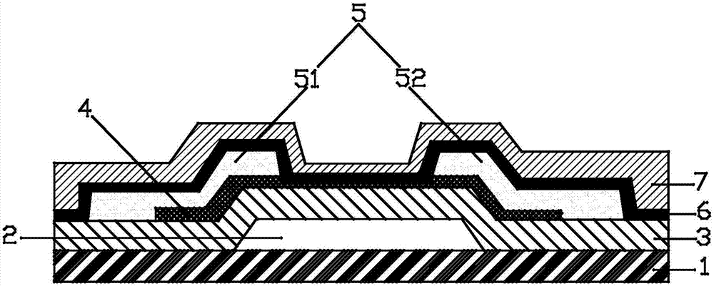
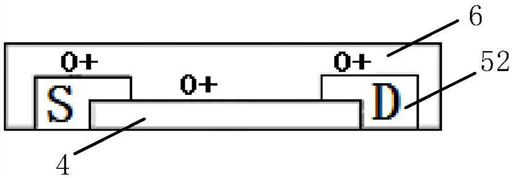
[0049] like Image 6 As shown, the formation of the isolation layer 6 covering the source-drain electrodes 5 and the channel region between the source-drain electrodes 5 specifically includes, under the environment of 170°C-200°C, SiH with a flow ratio of not less than 1:40 4 and N 2 O, formed by a plasma-enhanced chemical vapor deposition process including a thickness of isolation layer of silicon oxide compound. Due to the difference in performance of different devices, the actual process parameters for preparing the isolation layer 6 including the silicon oxide compound are different. In actual preparation, PECVD equipment can be used, the pressure is controlled at 70Pa-110Pa, the power is controlled at 800W-1500W, and the reaction temperature is 170°C-200°C, so that SiH 4 with N 2 O reaction, the deposition thickness on the sample surface is The isolation layer 6; according to different equipment, the deposition rate varies greatly, so the reaction time of the react...

Embodiment 2

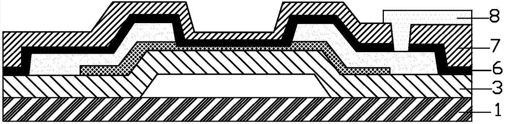
[0052] like Figure 8 As shown, the formation of the isolation layer covering the source-drain electrodes and the channel region between the source-drain electrodes specifically includes forming in an environment of 180°C-220°C through an atomic layer deposition process or a plasma-enhanced atomic layer deposition process. including a thickness of isolation layer of alumina. The reaction gas of alumina is trimethylaluminum gas and its oxidant. The specific operation can be: first pass trimethylaluminum gas, then purify with inert gas, and then pass in H 2 O, H 2 O plasma, O 2 Plasma, O 3 Wait for any source gas in the oxidant to carry out the evaporation reaction; the evaporation reaction can be repeated many times.

[0053] An atomic layer deposition chamber (ALD chamber) can be used for evaporating the aluminum oxide film layer. Due to the use of ALD technology, the deposition rate is relatively slow. Considering the efficiency of mass production, the evaporating thick...

Embodiment 3

[0058] like Figure 10 As shown, after the deposition of the active layer 4 and the source and drain electrodes 5 is completed, the source and drain electrodes 5 and the channel region between the source and drain electrodes 5 are first subjected to N 2 Oplasma treatment, and then use CVD equipment to vapor-deposit a layer of isolation layer 6; the isolation layer 6 is a silicon oxide compound with low temperature and low oxygen content, and its reaction gas includes SiH 4 and N 2 O, the SiH 4 and N 2 The ratio of O is not less than 1:40, and the evaporation temperature is 170°C-200°C. After completing the vapor deposition of the isolation layer 6, the isolation layer 6 is subjected to N for the second time. 2 Oplasma treatment. After the treatment, a silicon oxide compound with high oxygen content is deposited at a higher temperature as the passivation layer 7, specifically: using PECVD equipment, in an environment of 240°C-280°C, the flow ratio of SiH is not greater tha...


PUM


Abstract

The invention discloses a thin film transistor and a manufacturing method, and a display apparatus. The thin film transistor comprises a gate, a gate dielectric layer, an active layer, source and drain electrodes and a passivation layer; an isolation layer is arranged between the source and drain electrodes and the passivation layer; and the source and drain electrodes and a channel region between the source and drain electrodes are covered with the isolation layer. By evaporating the isolation layer on the source and drain electrodes and the channel region between the source and drain electrodes, the source and drain electrodes are not oxidized easily in the subsequent process, so that the problem of oxidization of copper in a subsequent high-temperature passivation process is relieved particularly.

Description

technical field [0001] The invention relates to the field of liquid crystal display, in particular to a thin film transistor, a manufacturing method and a display device. Background technique [0002] Oxide Thin Film Transistor (Oxide TFT for short) has become the first choice for the next-generation panel display industry due to its excellent electron mobility, good a-Si TFT production line compatibility and low-temperature manufacturing process. In recent years, with the increasingly fierce technical competition of domestic and foreign research institutes, the Oxide TFT process has entered the track of rapid mass production. [0003] In the back channel etching (BCE) structure of oxide thin film transistors, the treatment of the back channel region plays a very critical role. Usually, due to the damage to the back channel region by etching, conductors often appear in the active layer of the TFT. trend. Contents of the invention [0004] The main purpose of the present ...

Claims


Application Information

Patent Timeline
Patent Type & Authority Applications(China)
IPC IPC(8): H01L29/786H01L21/336H01L29/10H01L29/417
CPCH01L29/1033H01L29/41733H01L29/66742H01L29/78603H01L29/78621H01L27/1248H01L27/1218H01L27/1262H01L29/78618H01L33/44
Inventor 周天民杨维王利忠朱夏明宋吉鹏
Owner BOE TECH GRP CO LTD
Why Eureka
Try Eureka