
Diffusion process of silicon-wafer laser doping SE

A laser doping and diffusion process technology, used in photovoltaic power generation, sustainable manufacturing/processing, final product manufacturing, etc., can solve the problems of poor ohmic contact of silicon wafers, reduced cell efficiency, and poor ohmic contact, and achieves a solution to ohmic contact problems. bad contact effect

Inactive Publication Date: 2017-11-24
EGING PHOTOVOLTAIC TECHNOLOGY CO LTD
View PDF5 Cites 20 Cited by
  • Summary
  • Abstract
  • Description
  • Claims
  • Application Information

AI Technical Summary

Problems solved by technology

[0003] The technical problem to be solved by the present invention is: in the SE technology, the higher the square resistance, the higher the opening voltage and current, but the higher the square resistance, the less the phosphorus source diffuses, which will be caused by the phosphorus source during laser ablation. Insufficiently, the ablation area does not form a good heavy doping, which leads to poor ohmic contact, a decrease in fill factor, and a decrease in cell efficiency. In order to overcome the deficiencies in the prior art, the present invention provides a silicon wafer laser-doped SE Diffusion process to solve the technical problem of insufficient PSG concentration on the surface of the silicon wafer due to the high square resistance of the diffusion process in the existing laser SE technology, which eventually leads to poor ohmic contact in the heavily doped area of ​​the silicon wafer.

Method used


Image

  • Diffusion process of silicon-wafer laser doping SE

Examples


Embodiment Construction

[0017] A silicon wafer laser-doped SE diffusion process, the preparation process of the silicon wafer: including sequentially cleaning the silicon wafer, diffusion, laser doping, phosphorus washing, back passivation, front coating of the silicon wafer, and backside of the silicon wafer Coating, laser drilling and screen printing.

[0018] Wherein the diffusion process has the following steps:

[0019] 1. Put the cleaned silicon wafer on the quartz boat and push it into the diffusion furnace, and the temperature in the furnace rises to 770°C;

[0020] 2. Perform pre-oxidation pretreatment on the surface of the silicon wafer in the diffusion furnace, and the treatment time is 10 minutes;

[0021] 3. Introduce nitrogen carrying POCl3 into the diffusion furnace to deposit the first layer of phosphorus source. The deposition time is 10 minutes, and the temperature in the furnace is raised to 790°C;

[0022] 4. Stop feeding the nitrogen gas carrying POCl3, and raise the temperatur...


PUM


Abstract

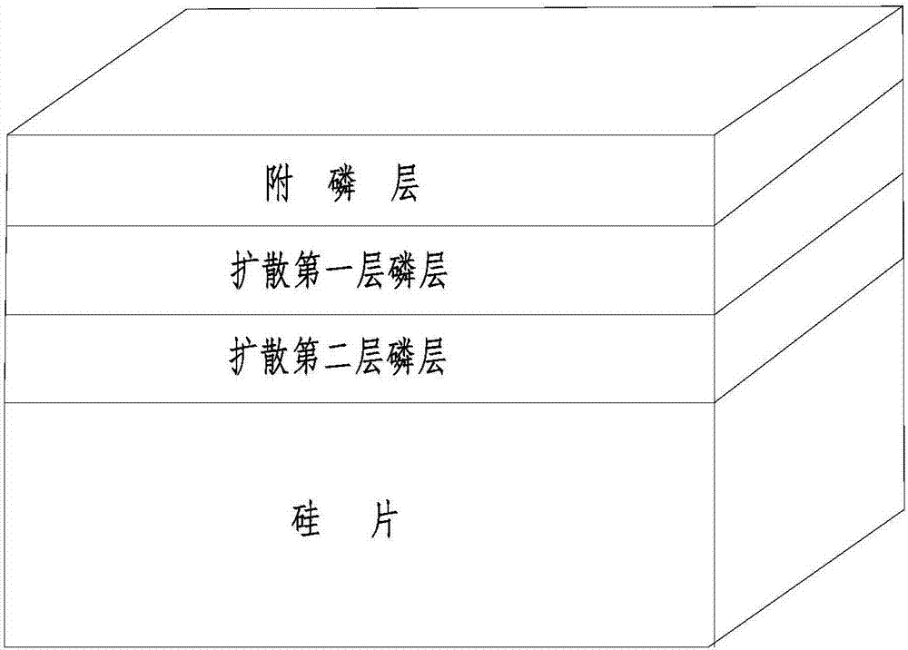
The invention relates to a diffusion process of a silicon-wafer laser doping SE. According to the process, after formation of a diffusion first phosphorus layer and a diffusion second phosphorus layer on a surface of a silicon wafer, phosphorus attachment layer deposition processing is carried out to form a phosphorus attachment layer on the surface of the silicon after diffusion. With the phosphorus attachment layer, a problem of insufficient PSG concentration of laser ablation is solved; the phosphorus attachment layer is easy to remove during the follow-up phosphorus washing and removing process and thus the low-surface-concentration lightly-doped region is kept at the emitter, so that problems of poor ohmic contact and packing factor reduction caused by low PSG concentration during laser doping are solved.

Description

technical field [0001] The invention relates to the technical field of solar cell preparation, in particular to a diffusion process for silicon wafer laser doping SE. Background technique [0002] In the current field of solar cell technology, the application of high-efficiency cell technology is constantly improving. For example, high-efficiency cells such as PERC have continuously improved their conversion efficiency. In the continuous stacking technology, one of them can be doped with laser to prepare selective emission. Electrode (SE) cells. The preparation of SE cells mainly has two characteristics: 1) the contact area between the metal grid line and the silicon wafer is a heavily doped area, which can form a good ohmic contact and improve the fill factor; 2) the light receiving area is a lightly doped area, which can improve Short-wave response, low surface concentration reduces the recombination of minority carriers, thereby increasing the open circuit voltage and sh...

Claims


Application Information

Patent Timeline
IPC IPC(8): H01L31/18H01L21/225H01L31/068
CPCH01L21/2252H01L31/068H01L31/1804Y02E10/547Y02P70/50
Inventor 刘阳
Owner EGING PHOTOVOLTAIC TECHNOLOGY CO LTD
Learn More