A laterally diffused metal oxide semiconductor ldmos device and its layout
An oxide semiconductor and device technology, applied in semiconductor devices, electrical components, circuits, etc., can solve problems such as device failure, and achieve the effect of weakening the electric field concentration effect, improving market competitiveness, and improving product reliability.
- Summary
- Abstract
- Description
- Claims
- Application Information
AI Technical Summary
Problems solved by technology
Method used
Image

Examples
no. 1 example
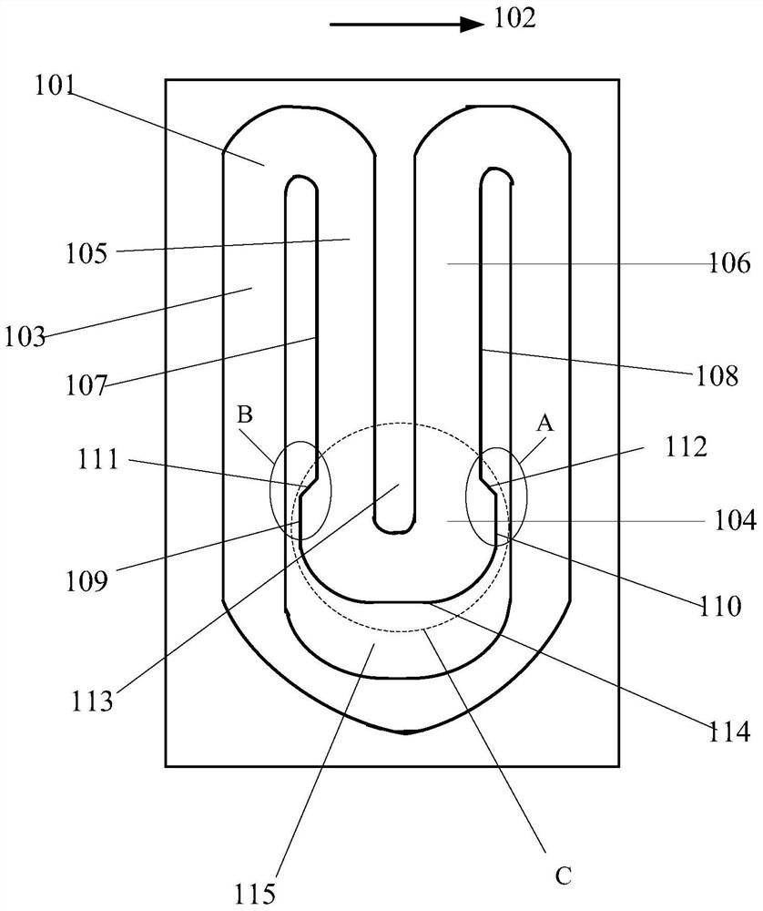
[0047] see figure 1 , the first embodiment of the present invention provides a laterally diffused metal oxide semiconductor LDMOS device, including: a P-type substrate;
[0048] A depletion region 101 formed on a P-type substrate;
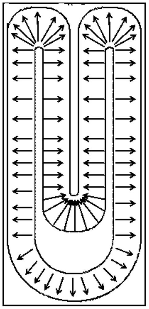
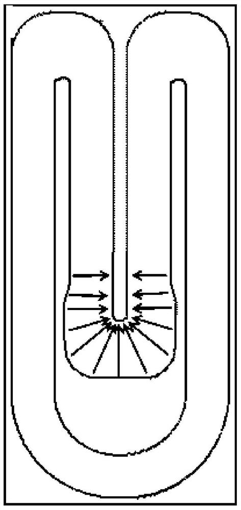
[0049] The depletion region 101 includes at least two straight regions 103 arranged in sequence along the first direction 102 and a transition region 104 connecting the two straight regions 103 at one end of the straight region 103, the transition region 104 is usually an electric field concentration region; wherein,
[0050]The two straight areas 103 include: a first straight area 105 and a second straight area 106, the distance between the first boundary 107 of the first straight area 105 and the second boundary 108 of the second straight area 106 is the first preset Assuming a distance, the first boundary 107 is a boundary away from the second straight region 106, and the second boundary 108 is a boundary far away from the first straight region...
no. 2 example
[0061] see Figure 7 , the second embodiment of the present invention provides a layout structure of a laterally diffused metal oxide semiconductor LDMOS device, including a depletion region 201 corresponding to the depletion region of the LDMOS device, specifically, the depletion region is transparent Photoregion for local selective oxidation (LOCOS) of LDMOS devices.
[0062] The depletion region portion 201 includes at least two straight region portions 203 arranged in sequence along the first direction and a transition region portion 204 connecting the two straight region portions 203 at one end of the straight region portion 203; wherein,
[0063] The two straight area portions 203 are respectively a first straight area portion 205 and a second straight area portion 206, and the distance between the first boundary of the first straight area portion 205 and the second boundary of the second straight area portion 206 is The first preset distance, the first boundary is the ...
no. 3 example
[0075] The third embodiment briefly describes the process flow of the LDMOS device provided by the present invention as follows:
[0076] first step, see Figure 7 , On the P-type 100 crystal orientation 80ohm-cm resistivity substrate (P sub), firstly use the local oxidation LOCOS process to make field oxygen (FOX).
[0077] The second step, see Figure 8 , sequentially perform photolithography, implantation, glue removal, and well pushing on the substrate to form the device depletion region (HVNW) and channel region (PW).
[0078] The third step, see Figure 9 , performing polycrystalline (POLY) deposition, photolithography, and etching in sequence to form a gate (Gate) region.
[0079] The fourth step, see Figure 10 , perform source (Source) N+ and Drain contact N+ implantation to form the core cross-sectional structure of LDMOS. In the cross-sectional structure, A is the depletion region, 700V products are usually 65um, and B is the Drain contact region.
PUM
 Abstract
Description
Claims
Application Information
 - R&D
- Intellectual Property
- Life Sciences
- Materials
- Tech Scout
- Unparalleled Data Quality
- Higher Quality Content
- 60% Fewer Hallucinations
Browse by: Latest US Patents, China's latest patents, Technical Efficacy Thesaurus, Application Domain, Technology Topic, Popular Technical Reports.
© 2025 PatSnap. All rights reserved.Legal|Privacy policy|Modern Slavery Act Transparency Statement|Sitemap|About US| Contact US: help@patsnap.com