Wafer-level fan-out type stack package process method

A packaging process, fan-out technology, applied in the manufacturing of electrical components, electric solid state devices, semiconductor/solid state devices, etc., can solve the problems of high manufacturing cost and complex process, save material costs, reduce manufacturing costs, and simplify manufacturing The effect of the process method

Active Publication Date: 2017-12-15
NAT CENT FOR ADVANCED PACKAGING
View PDF5 Cites 9 Cited by
  • Summary
  • Abstract
  • Description
  • Claims
  • Application Information

AI Technical Summary

Problems solved by technology

[0005] Therefore, the technical problem to be solved by the present invention is to overcome the defects of high manufacturing cost and complicated process of fan-out stack packaging in the prior art, thereby providing a wafer-level fan-out stack packaging process method

Method used


Image

  • Wafer-level fan-out type stack package process method
  • Wafer-level fan-out type stack package process method
  • Wafer-level fan-out type stack package process method

Examples


Embodiment 1

[0039]Embodiment 1 provides a wafer-level fan-out stack packaging process method, such as figure 1 As shown, it includes the following steps:

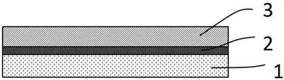
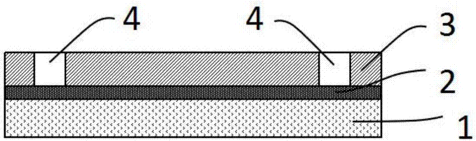
[0040] Step S1: Paste a layer of dry photoresist film 3 on the high-temperature bonding adhesive layer 2 on the light-transmitting temporary substrate 1 . The high-temperature bonding adhesive layer 2 can be cured at a lower temperature and has a stronger adhesive force. When the material is heated to a higher temperature, such as higher than 300°C, the interface between it and the light-transmitting temporary substrate 1 Can lose stickiness. The total thickness of the high-temperature bonding adhesive layer 2 is generally less than 10 μm. The high-temperature bonding adhesive layer 2 can be attached to the surface of the light-transmitting temporary substrate 1 by means of spray coating, spin coating, or film sticking. A layer of dry photoresist film 3 is pasted on the surface of the high-temperature bonding adhesive layer 2, and t...

Embodiment 2

[0055] Embodiment 2 provides a process method of wafer-level fan-out stack packaging, which includes all the steps of embodiment 1, and will not be repeated here to avoid repetition. Embodiment 2 discloses a specific method for stacking more than two packaging units to obtain a fan-out stacked packaging structure, that is, using the micro-bumps of the rewiring layer on the upper packaging unit 21 to interfere with the solidification on the lower packaging unit 22 adjacent to it. The conductive metal pillars exposed on the final dry photoresist film to realize the stacking of package units, such as Figure 13 shown.


PUM


Abstract

The invention discloses a wafer-level fan-out type stack package process method, and the method comprises the following steps: pasting a dry photoresistive membrane on a high-temperature bonding glue layer on a light-transmitting temporary substrate; forming a plurality of blind holes, which are directly communicated with the high-temperature bonding glue layer, on the dry photoresistive membrane; implanting conductive metal poles in the blind holes after the dry photoresistive membrane is solidified; pasting an unpacked chip on the surface of the dry photoresistive membrane; carrying out the integrated injection moulding, and carrying out the grinding of the surface of a plastic packaged body till the bonding pad of the unpacked chip is completely exposed; manufacturing a rewiring layer, used for connecting the conductive metal poles and the unpacked chip, on the grinding surface of the plastic packaged body, wherein the rewiring layer is provided with miniature salient points obtained through reballing and reflow soldering; removing the light-transmitting temporary substrate and the high-temperature bonding glue layer, and obtaining a package unit; and obtaining a fan-out stacked package structure according to the package unit. The method simplifies the manufacturing technology of a fan-out type stack package, and reduces the manufacturing cost of the stack package.

Description

technical field [0001] The invention relates to the technical field of semiconductor packaging, in particular to a wafer-level fan-out stack packaging process method. Background technique [0002] With the increasing integration of electronic devices, a stacked semiconductor packaging technology (Package on Package, PoP for short) and a stacked die package technology (Stacked Die Package) have been proposed in the field of semiconductor packaging. In this type of package, multiple packages or bare chips are overlapped in the height direction to reduce the footprint of the package. [0003] At present, the chip stacking PoP commonly used mostly adopts the packaging method of wire bond or flip chip (Flip chip) on the redistribution substrate. First, reserve pads or holes through the plastic film on the bottom substrate, and then use wire bond (WB for short) or Flip-Chip (FC for short) or a combination of the two to package the chip on the upper layer. The method realizes the...

Claims


Application Information

Patent Timeline
Patent Type & Authority Applications(China)
IPC IPC(8): H01L21/56H01L21/60
CPCH01L21/56H01L24/64H01L21/568H01L2224/04105H01L2224/12105H01L2224/19H01L2224/32225H01L2224/48235H01L2224/73265H01L2224/73267H01L2224/92244
Inventor 姚大平宋涛
Owner NAT CENT FOR ADVANCED PACKAGING
Why Eureka
Try Eureka