Transient voltage suppressor and manufacturing method therefor

A technology of transient voltage suppression and manufacturing methods, which is applied in semiconductor/solid-state device manufacturing, electric solid-state devices, circuits, etc., can solve the problems that multiple groups of chips cannot be packaged at the same time, increase packaging defects, increase the overall size, etc., and achieve product Stable parameters and performance, reduced processing difficulty, and high integration

Pending Publication Date: 2017-12-29
BEIJING YANDONG MICROELECTRONICS
View PDF5 Cites 2 Cited by
  • Summary
  • Abstract
  • Description
  • Claims
  • Application Information

AI Technical Summary

Problems solved by technology

However, the TVS device obtained by this method requires more than two groups of chips to be packaged in parallel, and two chips need to be placed on one of the substrates, which increases the possibility of packaging defects and increases the cost of packaging.
And because the integrated packaging of multiple chips requires more space and increases the overall size, for smaller packages, multiple groups of chips cannot be packaged at the same time

Method used


Image

  • Transient voltage suppressor and manufacturing method therefor
  • Transient voltage suppressor and manufacturing method therefor
  • Transient voltage suppressor and manufacturing method therefor

Examples


Embodiment Construction

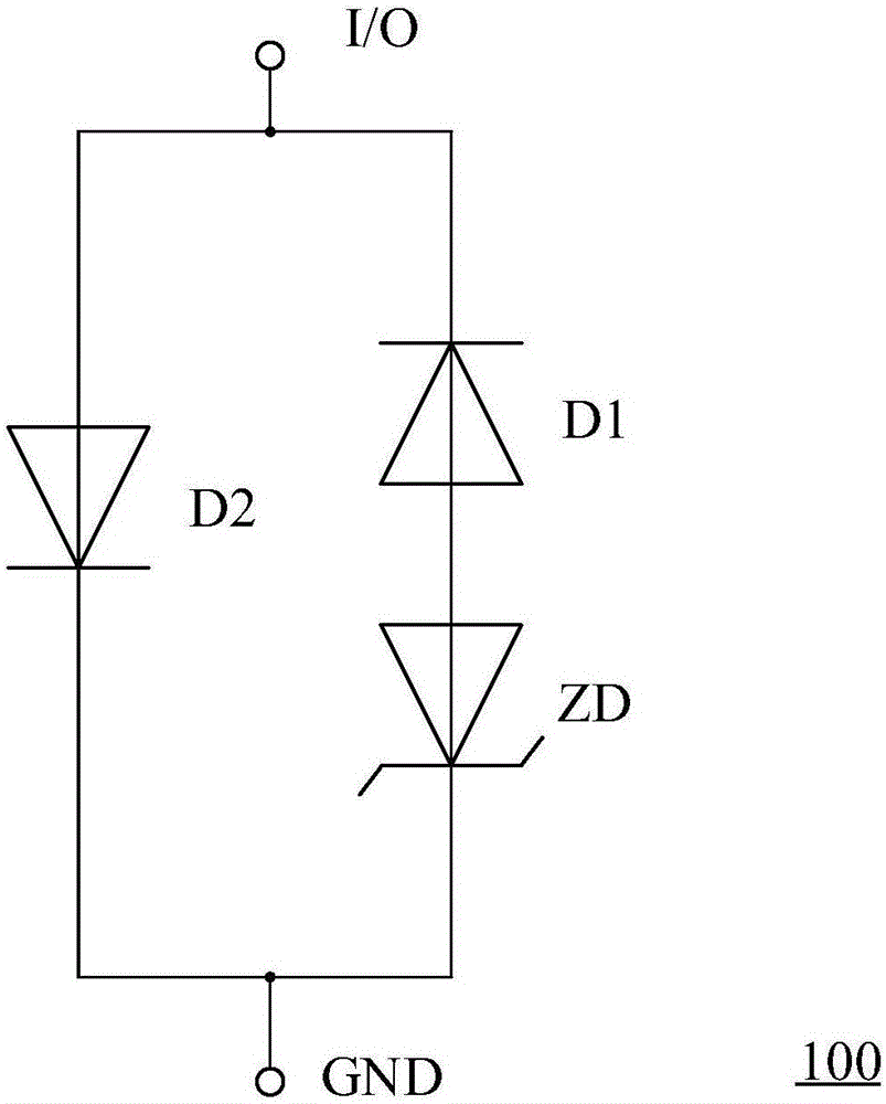
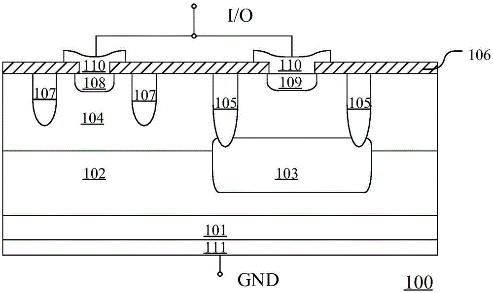
[0026] The present invention is described below based on examples, but the present invention is not limited to these examples. In the following detailed description of the embodiments of the present invention, some specific details are described in detail, and those skilled in the art can fully understand the present invention without the description of these details. In order to avoid obscuring the essence of the present invention, well-known methods, procedures, and flow charts are not described in detail.

[0027] In the various figures, identical elements are indicated with similar reference numerals. For the sake of clarity, various parts in the drawings have not been drawn to scale. Also, some well-known parts may not be shown in the drawings. The flowcharts and block diagrams in the accompanying drawings illustrate the possible system framework, functions and operations of the systems, methods, and devices of the embodiments of the present invention, and the blocks an...


PUM


Abstract

The invention discloses a transient voltage suppressor and a manufacturing method therefor. The transient voltage suppressor comprises a semiconductor substrate; a first epitaxial layer located on the first surface of the semiconductor substrate; a buried layer located in the epitaxial layer; a second epitaxial layer located on the first epitaxial layer; a first isolating region and a second isolating region which respectively extend from the surface of the second epitaxial layer to the interior of the buried layer and the interior of the second epitaxial layer, wherein the first and second isolating regions are respectively used for forming a first active region and a second active region in the second epitaxial layer; a first doping region and a second doping region, which are respectively located in the first active region and the second active region and extend to the interior of the second epitaxial layer from the surface of the epitaxial layer, wherein the first and second doping regions are in electrical connection. The doping type of the substrate is the same as the doping type of the epitaxial layer. The transient voltage suppressor enables a power device which occupies a large area to be made in a core, improves the utilization rate of the area of the chip and the integration degree, further reduces the size of the chip, and reduces the packaging cost.

Description

technical field [0001] The present invention relates to a semiconductor device and a manufacturing method thereof, more particularly, to a transient voltage suppressor and a manufacturing method thereof. Background technique [0002] Transient Voltage Suppressor (Transient Voltage Suppressor, TVS) is a device used to protect integrated circuits from overvoltage damage. The designed integrated circuits work in the normal range of voltage. However, Electrostatic Discharge (Electronic Static Unpredictable and uncontrollable high voltages generated by accidents such as Discharge (ESD), electrical fast transients, and lightning will cause damage to circuits. When such high voltages are generated, TVS devices are required to protect integrated circuits to avoid these possibilities Conditions that could damage the integrated circuit. [0003] The consumer electronics market is developing rapidly, and the performance of electronic products represented by mobile phones and mobile te...

Claims


Application Information

Patent Timeline
Patent Type & Authority Applications(China)
IPC IPC(8): H01L27/02H01L29/861H01L21/329
CPCH01L27/0255H01L29/6609H01L29/861
Inventor 周源郭艳华李明宇张欣慰
Owner BEIJING YANDONG MICROELECTRONICS
Why Eureka
Try Eureka