
1.5T depletion-type SONOS non-volatile memory and manufacturing method therefor

A non-volatile, manufacturing method technology, applied in the direction of electric solid-state devices, semiconductor devices, electrical components, etc., can solve the problem of large leakage current, uneven doping of the channel region, reduction of carrier mobility and junction characteristics And other issues

Active Publication Date: 2017-12-29
SHANGHAI HUAHONG GRACE SEMICON MFG CORP
View PDF3 Cites 9 Cited by
  • Summary
  • Abstract
  • Description
  • Claims
  • Application Information

AI Technical Summary

Problems solved by technology

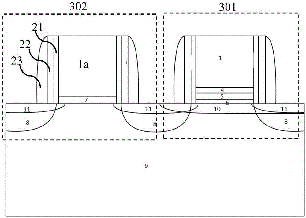
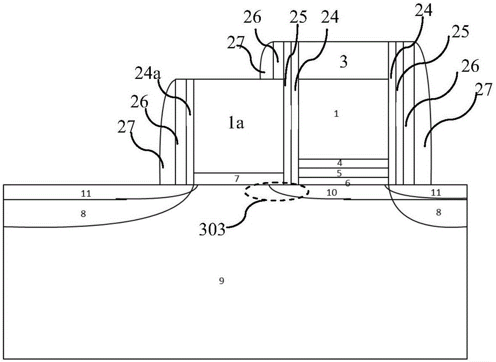
[0022] It can be seen from the above existing manufacturing process that the P-type substrate in the channel region of the selection tube needs to be repeatedly doped, which increases the complexity of the process and degrades device characteristics such as reducing carrier mobility and junction characteristics. Repeated doping makes the channel region of the selector tube doped unevenly. For the structure of unevenly doped channel region, please refer to Figure 4 as shown, Figure 4 , the doping of the channel region at the bottom of the polysilicon gate 1a is shown as a dotted circle 301, and it can be seen that the doping profile of the channel region of the selector is triangular. Figure 4 Different colors are used in the original figure to indicate different doping concentrations, such as Figure 4 Shown in DopingConcentration(NetActive)[cm^-3]
The triangular profile structure of the channel region may lead to a relatively large leakage current
In order to obtain better performance, the Vt implantation of SG needs to be specially optimized, so it will increase the complexity of the process

Method used


Image

  • 1.5T depletion-type SONOS non-volatile memory and manufacturing method therefor
  • 1.5T depletion-type SONOS non-volatile memory and manufacturing method therefor
  • 1.5T depletion-type SONOS non-volatile memory and manufacturing method therefor

Examples


Embodiment Construction

[0073] Such as Figure 5 Shown is a cell structure diagram of the 1.5T depletion-type SONOS non-volatile memory according to the embodiment of the present invention; the cell structure of the 1.5T depletion-type SONOS non-volatile memory according to the embodiment of the present invention includes a SONOS memory transistor and a selection transistor. Figure 5 It also shows a CMOS device integrated with a 1.5T depletion-mode SONOS non-volatile memory. CMOS devices are generally used as logic devices, including PMOS transistors and NMOS transistors. Figure 5 An NMOS tube is shown in .

[0074] The SONOS memory transistor and the selection transistor of the same cell structure share the same N-type doped channel region 102 formed on the surface of the P-type semiconductor substrate 101 . Preferably, the P-type semiconductor substrate 101 is a P-type silicon substrate.

[0075] The gate structure of the SONOS memory transistor includes an ONO layer and a first polysilicon gat...


PUM


Abstract

The invention discloses a 1.5T depletion-type SONOS non-volatile memory. A memotron and a selectron share one N-type doped channel region. The polysilicon gates of the memotron and selectron are isolated through a side wall. A trench is formed by the series connection of a first trench part covered by a first polysilicon gate of the memotron and a second trench part covered by a second polysilicon gate of the selectron. The first polysilicon gate is of an N+ doped type, thereby enabling a threshold voltage of the first trench part to be less than 0V. The second polysilicon gate is of a P+ doped type, and a threshold voltage of the second trench part is increased to a value greater than 0V through the feature that a work function of P+ doping is larger, thereby forming a structure where the memotron is of a depletion type and a selection transistor is of an enhanced type, and improving the uniformity and consistency of the trench through the shared trench injection. The invention also discloses a manufacturing method for the 1.5T depletion-type SONOS non-volatile memory. The technology can be simplified, and the performances of a device can be improved.

Description

technical field [0001] The invention relates to the field of semiconductor integrated circuit manufacturing, in particular to a 1.5T depletion-type SONOS non-volatile memory; the invention also relates to a 1.5T depletion-type SONOS non-volatile memory and a manufacturing method thereof. Background technique [0002] SONOS (Silicon-Oxide-Nitride-Oxide-Silicon) non-volatile memory with low operating voltage and better CMOS process compatibility is widely used in various embedded electronic products such as financial IC cards, automotive electronics and other applications. At present, the commonly used memory cell structure consists of a complete SONOS memory transistor and a complete select-gate (SG) to form a 2-transistor structure (2 transistors, 2T), that is, a 2T-type SONOS non-volatile memory. Each transistor has a complete The source, drain and gate, and the two transistors share a layer of polysilicon. The threshold voltage (Vt) of the SONOS memory transistor in the d...

Claims


Application Information

Patent Timeline
IPC IPC(8): H01L27/11568H01L29/10H01L29/423
CPCH01L29/1033H01L29/42356H10B43/30
Inventor 许昭昭钱文生胡君
Owner SHANGHAI HUAHONG GRACE SEMICON MFG CORP
Learn More