Preparation method of in-situ electrifying type indium arsenide/gallium antimonide superlattice semiconductor sample of transmission electron microscope

A transmission electron microscope sample and transmission electron microscope technology, applied in the preparation of test samples, etc., can solve the problems of low hardness and high difficulty in preparation of transmission electron microscope samples, and achieve the effect of huge application potential

Active Publication Date: 2018-01-12
FUDAN UNIV
View PDF6 Cites 3 Cited by
  • Summary
  • Abstract
  • Description
  • Claims
  • Application Information

AI Technical Summary

Problems solved by technology

Due to the low hardness of III-V compounds, it is difficult to prepare samples for transmission electron microscopy. In the past ten years, the microscopic research on III-V compounds in the literature has focused on static structu

Method used


Image

  • Preparation method of in-situ electrifying type indium arsenide/gallium antimonide superlattice semiconductor sample of transmission electron microscope
  • Preparation method of in-situ electrifying type indium arsenide/gallium antimonide superlattice semiconductor sample of transmission electron microscope
  • Preparation method of in-situ electrifying type indium arsenide/gallium antimonide superlattice semiconductor sample of transmission electron microscope

Examples


Embodiment Construction

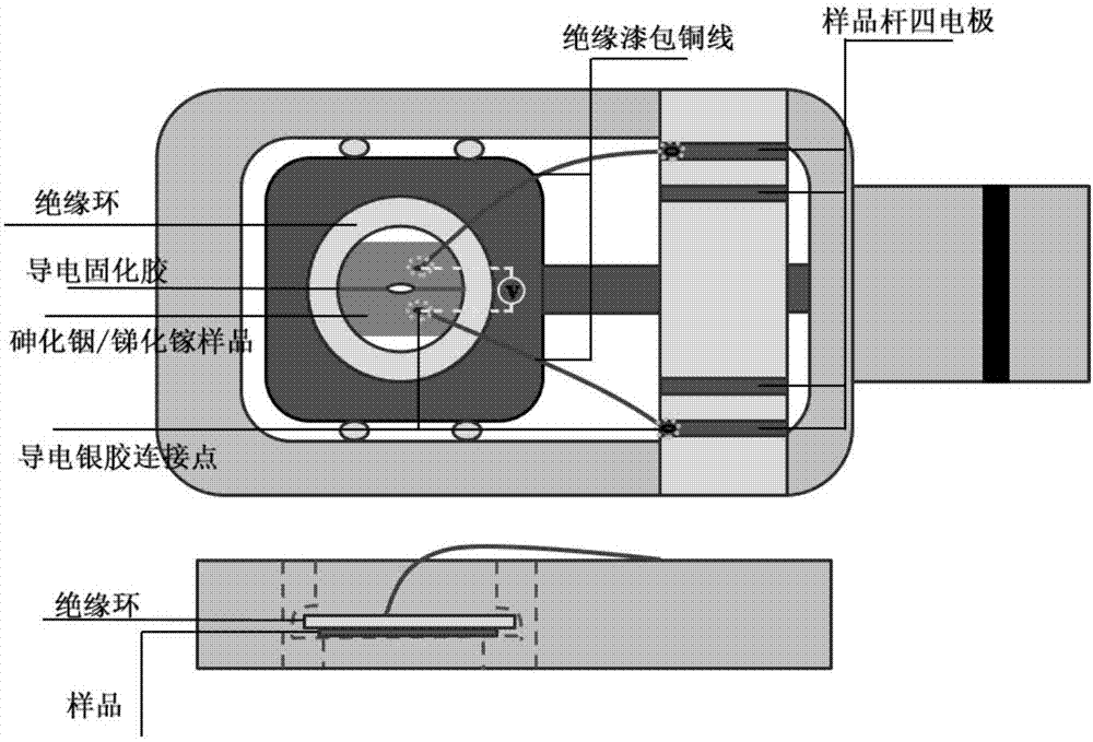
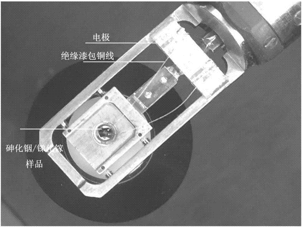
[0027] (1) Preparation of high temperature curing conductive silver glue

[0028] First, take the resin (Resin) and the curing agent (Hardender) in the commercial high-temperature curing glue, and mix them well at room temperature according to the ratio of 10:1~9:1; take an appropriate amount of commercial conductive silver glue according to the size of the sample, and mix with A small amount of high-temperature curing adhesive should be fully mixed according to the ratio of 3:1~3:2 for further use. It is worth noting that the prepared high-temperature curing conductive silver adhesive should be used as soon as possible, and should not exceed 24 hours at room temperature.

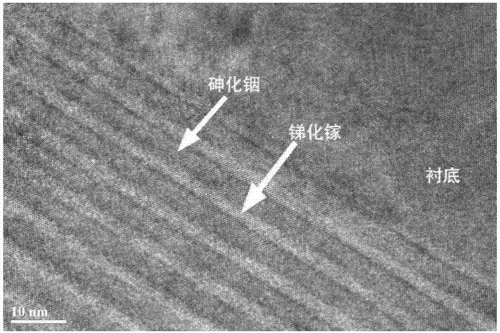
[0029] (2) TEM sample preparation of superlattice semiconductors

[0030] First, use a diamond knife to cut the bulk material into strips with a width of about 4-5 mm along the cleavage plane of the gallium antimonide substrate on which the superlattice semiconductor bulk material is grown, and then use a d...


PUM


Abstract

The invention belongs to the technical field of nanometer functional materials, and specifically relates to a preparation method of an of in-situ electrifying type indium arsenide/ gallium antimonidesuperlattice semiconductor sample of a transmission electron microscope. The preparation method comprises three steps of preparing high-temperature conductive adhesive, preparing a superlattice material transmission sample, and preparing an in-situ electrode, wherein the indium arsenide/ gallium antimonide superlattice semiconductor sample suitable for the characterization test of the transmissionelectron microscope can be prepared by oppositely adhering the conductive adhesive, and mechanically thinning and other processes, and then the sample is connected to a four-electrode transmission electron microscope sample stand through an enamel insulated wire, therefore, the in-situ electrifying test of the transmission electron microscope can be carried out. According to the preparation method, an arsenide/ gallium antimonide superlattice semiconductor is a classic and practical infrared photoelectric detecting device for researching the physical mechanism between a microstructure and current carrier property and the conveying mechanism of a current carrier in an electrifying working state, and the arsenide/ gallium antimonide superlattice semiconductor assists the design of photoelectric devices such as an infrared detector and a quantum cascade laser.

Description

technical field [0001] The invention belongs to the technical field of nanometer functional materials, and in particular relates to a method for preparing a sample of a superlattice semiconductor body material by applying an electric field in situ for a transmission electron microscope. Background technique [0002] III-V compound superlattice semiconductor is a mature and classic infrared detection device and imaging device. Based on its advantages such as wide detection range, flexible energy band adjustment and low dark current, III-V compound superlattice semiconductors have been widely studied by domestic and foreign scholars. 1-3 . Among them, indium arsenide, gallium antimonide, aluminum antimonide, and indium antimonide have similar lattice constants, and they have become the main choice for structure design and regulation. 4 . In recent years, in order to continuously improve the quantum efficiency of III-V compound superlattice semiconductors or reduce the dark ...

Claims


Application Information

Patent Timeline
IPC IPC(8): G01N1/28
Inventor 车仁超毕寒赵云昊刘璐赵雪冰张捷
Owner FUDAN UNIV
Why Eureka
Try Eureka