Fin field effect transistor and forming method thereof

A fin-type field effect transistor and fin technology, which are applied in the direction of electrical components, circuits, semiconductor devices, etc., to achieve the effect of improving electrical performance and high mobility

Active Publication Date: 2018-01-16
SEMICON MFG INT (SHANGHAI) CORP +1
View PDF10 Cites 3 Cited by
  • Summary
  • Abstract
  • Description
  • Claims
  • Application Information

AI Technical Summary

Problems solved by technology

[0005] However, the performance of the fin field effect tra

Method used


Image

  • Fin field effect transistor and forming method thereof
  • Fin field effect transistor and forming method thereof
  • Fin field effect transistor and forming method thereof

Examples


Embodiment Construction

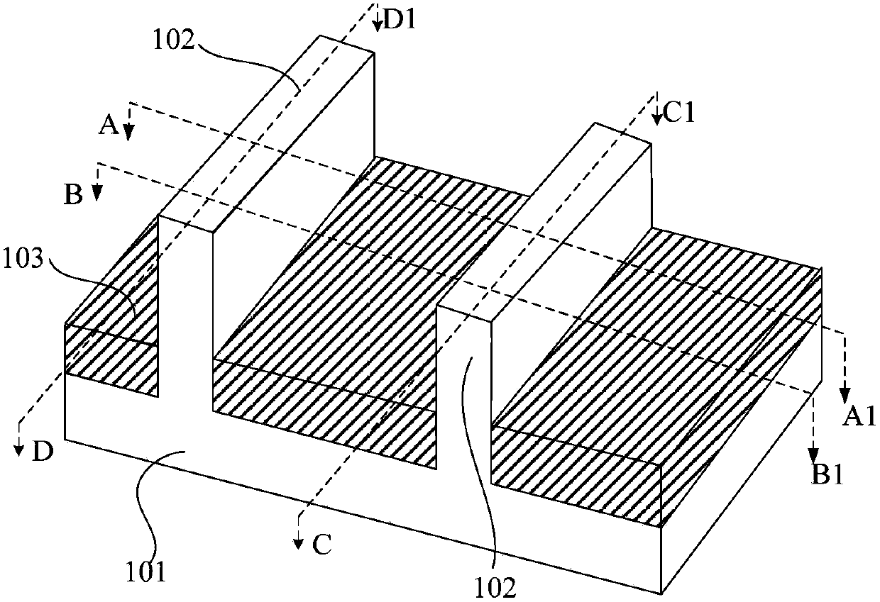
[0023] It can be known from the background technology that the electrical performance of the fin-type field effect transistor formed in the prior art needs to be improved, especially the electrical performance of the NMOS fin-type field effect transistor is poor.

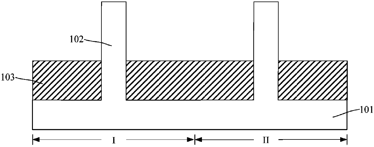
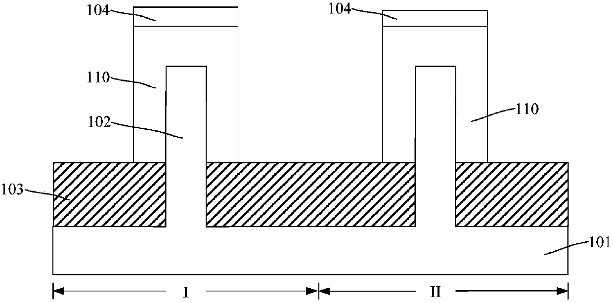
[0024] After analysis, the formation process of the NMOS fin-type field effect transistor includes the steps: forming a mask sidewall on the sidewall of the fin in the NMOS region; and etching and removing the fins of the thickness on both sides of the gate structure in the NMOS region. An N-zone groove is formed in the part; an N-type doped epitaxial layer filling the N-zone groove is formed. In order to limit the morphology and volume of the formed N region doped epitaxial layer, when the fins on both sides of the gate structure in the NMOS region are etched and removed, the mask sidewalls on the sidewalls of the fins are retained, so that the formation The two opposite sidewalls of the groove in the N region are mas...


PUM

PropertyMeasurementUnit
Thicknessaaaaaaaaaa

Abstract

The invention discloses a fin field effect transistor and a forming method thereof. The forming method comprises steps: a substrate comprising an NMOS area is provided, wherein convex fin parts are arranged on the substrate, isolation structures covering the side walls of the fin parts are arranged on the substrate, and the top part of the isolation structure is lower than the top part of the finpart; a gate structure is formed on the isolation structure and crosses the fin part; an N area mask lateral wall is formed on the fin part side wall in the NMOS area; the partial thickness of the finparts at two sides of the gate structure in the NMOS area is etched and removed, and the NMOS area fin part after etching and the N area mask lateral wall form an N area groove; an intrinsic blockinglayer is formed on the fin part exposed on the side wall of the N area groove; and an N-type doped epitaxial layer fully filling the N area groove is formed on the intrinsic blocking layer. Doped ions in the N-type doped epitaxial layer can be prevented from being diffused in a channel area below the gate structure, and the electrical performance of the formed fin field effect transistor is improved.

Description

Technical field [0001] The invention relates to the technical field of semiconductor manufacturing, in particular to a fin-type field effect tube and a forming method thereof. Background technique [0002] With the continuous development of semiconductor process technology, the development trend of semiconductor process nodes following Moore's Law continues to decrease. In order to adapt to the reduction of process nodes, the channel length of the MOSFET has to be continuously shortened. The shortening of the channel length has the advantages of increasing the die density of the chip and increasing the switching speed of the MOSFET field effect tube. [0003] However, as the channel length of the device is shortened, the distance between the source and drain of the device is also shortened. As a result, the gate's ability to control the channel becomes worse, and the gate voltage pinches off the channel. The difficulty of this is increasing, making the phenomenon of subthreshold ...

Claims


Application Information

Patent Timeline
IPC IPC(8): H01L29/06H01L29/78H01L21/8238H01L21/336
Inventor 李勇居建华
Owner SEMICON MFG INT (SHANGHAI) CORP
Why Eureka
Try Eureka