
High haze transparent conductive film and manufacturing method thereof

A technology of transparent conductive film and high haze, applied in the direction of conductive layer on insulating carrier, cable/conductor manufacturing, circuit, etc., can solve the problem of poor transmittance improvement effect, achieve strong adhesion, effective Good for storage and transportation, strong scattering effect

Inactive Publication Date: 2018-01-26
NINGBO INST OF MATERIALS TECH & ENG CHINESE ACADEMY OF SCI +1
View PDF10 Cites 2 Cited by
  • Summary
  • Abstract
  • Description
  • Claims
  • Application Information

AI Technical Summary

Problems solved by technology

Another example is the Chinese patent application with publication number CN103258865A, which discloses an oxide film substrate, its manufacturing method, photovoltaic cells and organic light-emitting devices including it. This application improves the haze value by forming textures on the oxide film. The application Also limited by the thickness of the oxide, these sub-wavelength scale structures are less effective in improving the transmittance

Method used


Image

  • High haze transparent conductive film and manufacturing method thereof
  • High haze transparent conductive film and manufacturing method thereof
  • High haze transparent conductive film and manufacturing method thereof

Examples


Embodiment 1

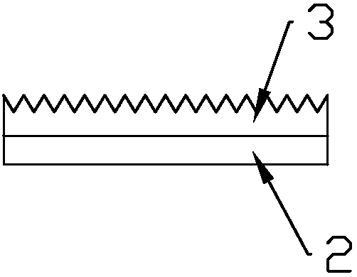
[0044] A silver grid transparent electrode with high haze random suede scattering, including a silver grid transparent electrode, one side of the silver grid transparent electrode is a smooth plane, and the other side is coated with ultraviolet glue with a random inverted pyramid structure .

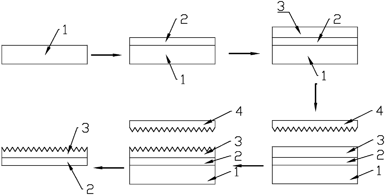
[0045] Such as figure 2 Shown, the preparation method of the transparent conductive film of above-mentioned high haze is as follows:

[0046] (1) preparing a layer of thickness on the silicon substrate as a 30nm silver grid transparent electrode;

[0047] (2) The method of spin coating is adopted to spin coat a layer of UV glue with a thickness of 300 μm on the surface of the silver grid transparent electrode, the rotating speed of spin coating is 400rpm, and the time of uniform glue is 60s;

[0048] (3) Lightly press the transparent PDMS template with a nanometer-sized random inverted pyramid structure into contact with UV glue, and irradiate it under a UV lamp for 1 min;

[0049] (4)...

Embodiment 2

[0063] An ultrathin metallic silver transparent electrode with high haze nanocone scattering, whose structure is as follows figure 1 As shown, it includes an ultra-thin silver transparent electrode, one side of the silver transparent electrode is a smooth plane, and the other side is coated with ultraviolet glue with a nanocone structure.

[0064] Such as figure 2 Shown, the preparation method of the transparent conductive film of above-mentioned high haze is as follows:

[0065] (1) preparing a layer of thickness on the silicon substrate as a 7nm ultra-thin silver transparent electrode;

[0066] (2) Adopting the method of spin coating, spin coating one deck thickness on the surface of silver transparent electrode is 500 μ m UV glue, the rotating speed of spin coating is 500rpm, and the time of uniform glue is 30s;

[0067] (3) Lightly press the transparent PDMS template with the nanocone structure into contact with the UV glue, and irradiate it under the UV lamp for 1 min;...

Embodiment 3

[0076] A silver nanowire transparent electrode with high haze random suede scattering, including a silver nanowire transparent electrode, one side of the silver nanowire transparent electrode is a smooth plane, and the other side is coated with ultraviolet glue with a random inverted pyramid structure .

[0077] Such as figure 2 Shown, the preparation method of the transparent conductive film of above-mentioned high haze is as follows:

[0078] (1) preparing a layer of thickness on the silicon substrate as a silver nanowire transparent electrode of 90nm;

[0079] (2) Adopt the method of spin-coating, on the surface of the transparent electrode of silver mesh, spin-coat a layer of thickness and be 1 μ m UV glue, the rotating speed of spin-coating is 8000rpm, and the time of uniform glue is 15s;

[0080] (3) Lightly press the transparent PDMS template with a nanometer-sized random inverted pyramid structure into contact with UV glue, and irradiate it under a UV lamp for 1 min...


PUM

PropertyMeasurementUnit
thicknessaaaaaaaaaa
electrical resistivityaaaaaaaaaa
reflectanceaaaaaaaaaa

Abstract

The invention discloses a high haze transparent conductive film and a manufacturing method thereof and relates to the transparent conductive electrode manufacturing field. The transparent conductive film comprises a transparent electrode, wherein one surface of the transparent electrode is coated with a transparent transfer printing medium with a suede surface. The manufacturing method comprises steps that the transparent electrode is made on a substrate, the surface of the electrode is uniformly coated with a transfer printing medium layer, the surface of the electrode coated with the transfer printing medium is made to tightly contact with a texturing template, after solidification, the transfer printing medium is separated from the texturing template, the electrode is separated from thesubstrate, and the high haze transparent conductive film is acquired. The high haze transparent conductive film is advantaged in that the conductive film has high haze, low reflectivity is realized,and stronger light scattering capability is realized, moreover, the haze and a water static contact angle value are adjustable. The manufacturing method is advantaged in that the method is simple andeasy.

Description

technical field [0001] The invention relates to the technical field of preparation of transparent conductive electrodes, in particular to a high-haze transparent conductive film and a preparation method thereof. Background technique [0002] Generally speaking, a transparent electrode means that the transmittance to the spectrum of the incident light wavelength range between 380nm and 780nm is greater than 80%, and the resistivity is lower than 10 -3 Ω·cm film electrode. Transparent electrodes are widely used in optoelectronic devices such as touch screens, displays, electromagnetic shielding, solar cells, and LEDs. At present, the main types of transparent electrodes are: indium tin oxide (ITO) transparent electrodes, carbon nanotube transparent electrodes, graphene transparent electrodes, metal nanowire transparent electrodes, metal grid transparent electrodes, etc. [0003] Haze is a very important performance parameter of transparent conductive film. Haze refers to the...

Claims


Application Information

Patent Timeline
Patent Type & Authority Applications(China)
IPC IPC(8): H01B5/14H01B13/00
Inventor 杨熹叶继春高平奇盛江肖剑峰黄志林夏金才周建宏
Owner NINGBO INST OF MATERIALS TECH & ENG CHINESE ACADEMY OF SCI
Learn More