A three-state charge trap memory based on graphene oxide quantum dots and its preparation method

A graphene quantum dot, charge trapping technology, applied in the direction of electric solid devices, circuits, electrical components, etc., can solve problems such as reducing operating voltage, achieve strong information storage capacity, stable data retention characteristics, stable flat-band voltage retention characteristics Effect

Active Publication Date: 2020-01-14
HEBEI UNIVERSITY
View PDF6 Cites 0 Cited by
  • Summary
  • Abstract
  • Description
  • Claims
  • Application Information

AI Technical Summary

Problems solved by technology

Although the operating voltage of these memories is still high, the charge-trapping layer using new materials achieves fast reading and writing and high stability of the memory, and there is still room for reducing the operating voltage

Method used


Image

  • A three-state charge trap memory based on graphene oxide quantum dots and its preparation method
  • A three-state charge trap memory based on graphene oxide quantum dots and its preparation method
  • A three-state charge trap memory based on graphene oxide quantum dots and its preparation method

Examples


Embodiment 1

[0037] Example 1 Three-state charge trap memory based on graphene oxide quantum dots

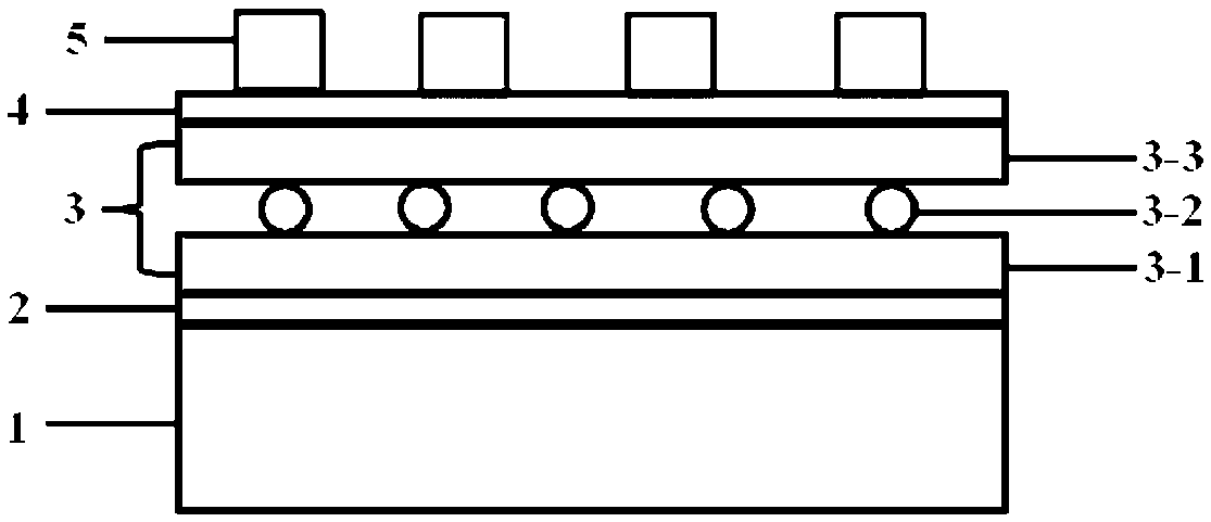
[0038] Such as figure 2As shown, the three-state charge trapping memory based on graphene oxide quantum dots of the present invention has a structure including the bottom substrate 1, an oxide dielectric layer on the substrate 1 and an electrode film layer 5 on the oxide dielectric layer, in,

[0039] The substrate 1 is a p-type Si substrate;

[0040] The oxide dielectric layer is a composite structure of a silicon dioxide tunneling oxide layer 2, a charge trapping layer 3 and a silicon dioxide blocking oxide layer 4, wherein the charge trapping layer 3 consists of the first zinc oxide film layer 3-1, A single-layer graphene oxide quantum dot layer 3-2 and a second zinc oxide film layer 3-3 are formed; wherein, the thickness of the silicon dioxide tunneling oxide layer 2 is 2 to 5 nm, and the thickness of the silicon dioxide blocking oxide layer 4 is 5-15nm, the thickness of the first zi...

Embodiment 2

[0042] Example 2 Preparation method of triple-state charge-trap memory based on graphene oxide quantum dots

[0043] (1) Forming an oxide dielectric layer on the substrate.

[0044] ①. Selection and processing of substrate materials

[0045] Select p-type Si (100 crystal orientation) as the substrate (or substrate), put the substrate in acetone and clean it ultrasonically for 10 minutes, then put it in alcohol and clean it ultrasonically for 10 minutes, then take it out and put it in Use ultrasonic cleaning in deionized water for 5 minutes, then take it out, and use nitrogen (N 2 ) and blow dry; then soak the substrate in a hydrofluoric acid solution diluted with deionized water, take it out and clean it again with ultrasonic waves in deionized water for 5 minutes, and then take it out with N 2 Blow dry to clean the treated Si substrate.

[0046] ② Growth of silicon dioxide tunneling oxide layer

[0047] Fix the cleaned Si substrate in a rapid thermal oxidation furnace. In...


PUM

PropertyMeasurementUnit
thicknessaaaaaaaaaa
thicknessaaaaaaaaaa
thicknessaaaaaaaaaa

Abstract

The invention provides a three-state charge capture memory based on graphene oxide quantum dots and a manufacturing method thereof. According to the memory, an oxide dielectric layer and a Pd electrode film layer are sequentially formed on a Si substrate; the oxide dielectric layer is formed by a silica tunneling oxide layer, a ZnO / GOQDs / ZnO charge capture layer and a silica blocking oxidization layer which are sequentially formed on the Si substrate, and GOQDs of the ZnO / GOQDs / ZnO charge capture layer is an oxidized graphene quantum dot layer. The memory is in a stable three-capacitance valuestate. Under the + / -4V operation voltage, a 1.86V storage window is presented; in the 104-second holding test time, capacitance values 1, 2 and 3 are relatively stable, stable data maintenance characteristics are presented, flat band voltage values during programming and erasion are relatively stable, and charge loss is only 8%. The method is advantaged in that excellent storage performance is consistent with development requirements of low operation voltage, high storage density and high stability in the present memory field.

Description

technical field [0001] The invention relates to a charge-trap memory, in particular to a three-state charge-trap memory based on graphene oxide quantum dots and a preparation method thereof. Background technique [0002] Nonvolatile memories (Nonvolatile Memories, NVM) have received great attention in the semiconductor memory industry. Non-volatile memory can store and read information in bytes. It has the advantages of high-density storage and low power consumption, and its reading and writing speeds are relatively fast. Part of non-volatile memory The speed can already approach DRAM. [0003] Among the existing nonvolatile memories, charge trapping memory (Charge Trapping Memory, CTM) is a widely used and important nonvolatile memory. The programming speed and erasing speed of the charge trap memory are relatively fast, and it has strong tolerance, can realize a high number of repeated operations, and can maintain data for a long time, and has good reliability. At the s...

Claims


Application Information

Patent Timeline
Patent Type & Authority Patents(China)
IPC IPC(8): H01L27/11568H01L29/51
Inventor 闫小兵贾信磊王宏杨涛
Owner HEBEI UNIVERSITY
Why Eureka
Try Eureka