A charge-trapping memory based on a single-layer barium strontium titanate thin film and its preparation method

A barium strontium titanate thin film and charge trapping technology, which is applied in the direction of electric solid-state devices, circuits, electrical components, etc., can solve the problems of poor fatigue resistance, small storage window, poor stability of high and low state capacitance and flat band voltage, etc. Excellent fatigue characteristics, fast switching speed, and stable maintenance characteristics

Active Publication Date: 2020-03-31
HEBEI UNIVERSITY
View PDF3 Cites 0 Cited by
  • Summary
  • Abstract
  • Description
  • Claims
  • Application Information

AI Technical Summary

Problems solved by technology

[0004] The object of the present invention is to provide a charge-trapping memory based on a single-layer barium strontium titanate film and its preparation method, to solve the problems of existing charge-trapping memories with poor stability of high and low state capacitance and flat band voltage, and relatively small storage window , poor fatigue resistance

Method used


Image

  • A charge-trapping memory based on a single-layer barium strontium titanate thin film and its preparation method
  • A charge-trapping memory based on a single-layer barium strontium titanate thin film and its preparation method
  • A charge-trapping memory based on a single-layer barium strontium titanate thin film and its preparation method

Examples


Embodiment 1

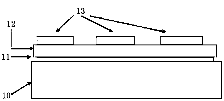
[0036] The structure of the charge trapping memory prepared by the present invention is as follows: figure 2 As shown, its structure from bottom to top is p-Si substrate 10, SiO 2 Tunneling layer 11 , BST trapping barrier layer 12 and Pd electrode layer 13 .

[0037] Wherein the p-Si substrate 10 is 100 crystal orientation; BST capture barrier layer 12 is grown on the p-Si substrate 10 by the method for magnetron sputtering, and its thickness is 5 ~ 100nm, under the preferred 10 ~ 50nm, its storage The window is bigger.

[0038] Of which SiO 2The tunneling layer 11 is formed by forming the BST trapping barrier layer 12 on the p-Si substrate 10 and then performing an annealing process. The annealing process refers to raising the temperature from room temperature to 600°C in an oxygen atmosphere for 20~40s. , keep warm for 2~10min, and then cool down from 600℃ to room temperature in 1~5min; the final formed SiO 2 The thickness of the tunneling layer is 2~4nm.

[0039] The ...

Embodiment 2

[0041] The preparation method of the resistive memory provided by the present invention comprises the following steps:

[0042] (1) Clean the p-type Si substrate (p-Si substrate) with 100 crystal orientation in acetone, alcohol and deionized water with ultrasonic wave for 5 minutes respectively, then take it out and put it into HF solution (the mass ratio concentration of HF and water is 3 :1) Clean in medium, take it out and wash it in deionized water, and finally take it out and use N 2 blow dry;

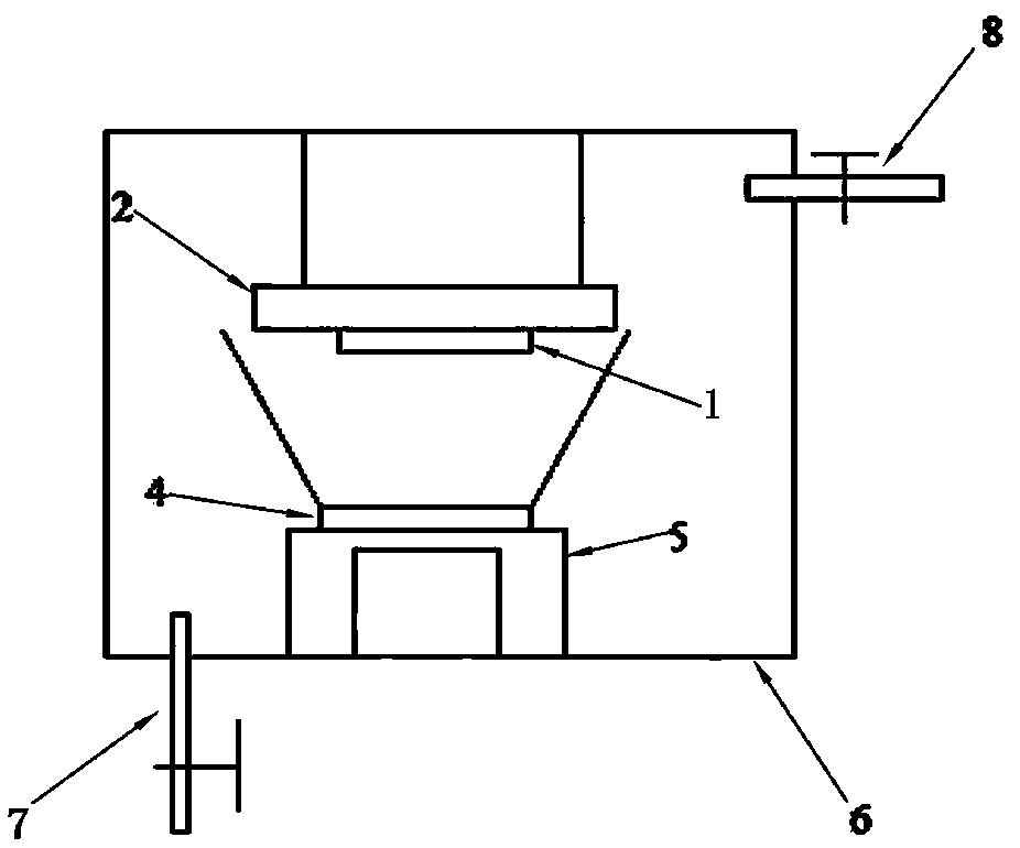
[0043] (2) using such as figure 1 In the shown magnetron sputtering equipment, a target stage 5 is arranged under the substrate stage 2 in the growth chamber 6, and a target material 4 is placed on the top of the target stage 5; the growth chamber 6 of the magnetron sputtering apparatus is opened, and the BST The target is fixed on the target stage 5 of the magnetron sputtering equipment, and the p-Si substrate is placed on the substrate holder 1 and then fixed on the substrate ...

Embodiment 3

[0047] Embodiment 3 performance test

[0048] The charge-trapping memory prepared in Example 2 was tested for performance, and its C-V curve is shown in Figure 4, and the storage window-scanning voltage characteristics are as follows Figure 5 shown. The figure shows that the scanning voltage starts to increase from 2V at a time. When the scanning voltage increases to 6V, that is, when the scanning voltage is +6V→-6V→+6V, the storage window of the storage device begins to open, and the storage device begins to have storage performance. As the scanning voltage increases, the storage window gradually increases. When the scanning voltage reaches 14V, it presents a large storage window of 8.1V, which indicates a very good storage effect.

[0049] The high and low state retention characteristics of the charge trapping memory prepared in embodiment 2 were measured, and the results are shown in Figure 6 .

[0050] The flat-band voltage retention characteristics of the charge-tra...


PUM

PropertyMeasurementUnit
thicknessaaaaaaaaaa
thicknessaaaaaaaaaa
thicknessaaaaaaaaaa

Abstract

The invention discloses a charge-trapping memory based on a single-layer barium strontium titanate (BST) thin film, and its structure is a P-type Si substrate, a SiO 2 tunneling layer, barium strontium titanate capture barrier layer and Pd electrode layer. At the same time, the preparation method of the memory is also disclosed. The P-type Si substrate is washed and dried, and a barium strontium titanate capture barrier layer is formed on the Si substrate by magnetron sputtering. SiO 2 tunneling layer, and then a Pd electrode layer was formed on the barium strontium titanate capture barrier layer by magnetron sputtering. The present invention prepares p-Si substrate / SiO through specific materials and methods 2 A charge-trapping memory with a composite structure of tunneling layer / barium strontium titanate trapping layer / Pd electrode layer. Tests show that, compared with the existing memory of the same type, the memory provided by the present invention has a larger storage window and better data retention, and is a memory device that is fatigue-resistant, has a fast writing / erasing rate, and has wider application prospects. of memory.

Description

technical field [0001] The invention relates to a memory device and a preparation method thereof, in particular to a charge-trap type memory based on a single-layer barium strontium titanate thin film and a preparation method thereof. Background technique [0002] Today's world is an information world, and information storage is ubiquitous, such as mobile phones, MP3, notebooks, U disks, etc. With the development of portable storage devices and cloud storage, people have higher and higher requirements for non-volatile memory. Therefore, the development of high-performance, low-power non-volatile memory will become the development trend of storage technology. Charge trapping memory (charge trapping memory, CTM) is a kind of non-volatile memory based on the change of high and low state capacitance value to record and store information. It has low power consumption, high charge storage density, fast writing, Erase rate, excellent data retention and excellent fatigue resistance...

Claims


Application Information

Patent Timeline
Patent Type & Authority Patents(China)
IPC IPC(8): H01L27/115
CPCH10B43/00
Inventor 闫小兵张园园赵建辉周振宇
Owner HEBEI UNIVERSITY
Why Eureka
Try Eureka