Diameter enlarging growth method of monocrystal diamond

A single crystal diamond and growth method technology, applied in the field of microelectronics, can solve problems such as hindering the effective diameter expansion of the upper surface of a single crystal epitaxial film, and achieve the effects of reducing the content of polycrystals, effective diameter expansion growth, and simple operation

Active Publication Date: 2018-02-09
湖州中芯半导体科技有限公司
View PDF9 Cites 12 Cited by
  • Summary
  • Abstract
  • Description
  • Claims
  • Application Information

AI Technical Summary

Problems solved by technology

[0004] 1. For a square substrate with (100) crystal planes on all four sides, the epitaxial film grown on it tends to have (113) crystal planes at the four corners, hindering the effective expansion of the upper surface of the single crystal epitaxial film;

Method used


Image

  • Diameter enlarging growth method of monocrystal diamond
  • Diameter enlarging growth method of monocrystal diamond

Examples


Embodiment 1

[0018] Example 1, based on an octagonal HPHT diamond substrate, a diamond epitaxial film with a (001) crystal plane and a thickness of 0.5 mm was grown.

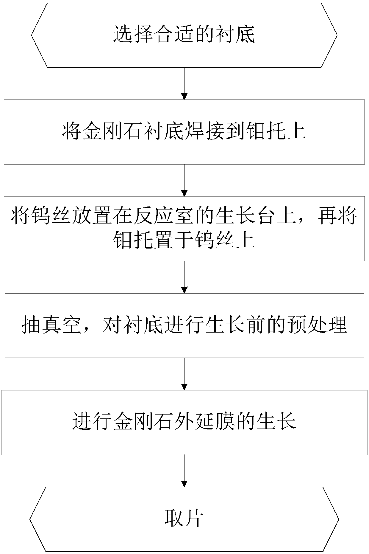
[0019] Step 1, select the substrate.

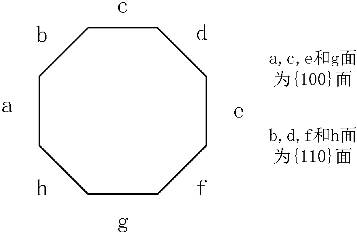
[0020] refer to figure 2 In this example, octagonal high-temperature and high-pressure HTHP diamond is selected as the substrate. The upper surface of the substrate is a (001) crystal plane, and the side surface is a {100} crystal plane alternated with a {110} crystal plane, that is, a plane, c plane, e plane The plane and g plane are {100} crystal planes, and the b, d, f and h planes are {110} crystal planes.

[0021] Step 2, welding the diamond substrate to the molybdenum support.

[0022] Place the molybdenum holder in the MPCVD reaction chamber, place a 25 μm thick gold foil on the molybdenum holder, and then place the selected high-temperature and high-pressure HPHT diamond substrate on the gold foil;

[0023] Evacuate the reaction chamber to a vacuum value of less than 10 -6 ...

Embodiment 2

[0030] Example 2, based on an octagonal HPHT diamond substrate, a diamond epitaxial film with a (001) crystal plane and a thickness of 1.2 mm was grown.

[0031] Step A, select the substrate.

[0032] The specific implementation of this step is the same as step 1 of Example 1.

[0033] Step B, welding the diamond to the molybdenum support.

[0034] Place a molybdenum holder in the MPCVD reaction chamber, place a 50 μm thick gold foil on the molybdenum holder, place the selected high-temperature and high-pressure HPHT diamond substrate on the gold foil, and vacuum the reaction chamber to make the vacuum degree of the reaction chamber less than 10 -6 mbar, the substrate is heated in the reaction chamber until the gold foil is melted, and the diamond substrate is welded to the molybdenum holder.

[0035] Step C, placing a tungsten wire with a diameter of 200 μm on the growth stage of the MPCVD reaction chamber, and placing the molybdenum holder welded with the substrate on the ...

Embodiment 3

[0041] Example 3, based on an octagonal HPHT diamond substrate, a diamond epitaxial film with a thickness of 2.5 mm and a (001) crystal plane was grown.

[0042] The implementation steps of this example are as follows:

[0043] Step 1, select the substrate.

[0044] The specific implementation of this step is the same as step 1 of Example 1.

[0045] Step 2: Place the molybdenum holder in the MPCVD reaction chamber, place the gold foil on the molybdenum holder, and then place the selected high-temperature and high-pressure HPHT diamond substrate on the gold foil. After the MPCVD reaction chamber is evacuated, the substrate is heated until the gold foil melts, and the diamond substrate is welded to the molybdenum support, wherein:

[0046] Gold foil thickness is 100μm;

[0047] The initial vacuum degree of the reaction chamber is less than 10 -6 mbar;

[0048] Step 3, place a tungsten wire with a diameter of 250 μm on the growth table of the MPCVD reaction chamber, and the...


PUM

PropertyMeasurementUnit
Thicknessaaaaaaaaaa

Abstract

The invention discloses a diameter enlarging growth method of monocrystal diamond. The diameter enlarging growth method of monocrystal diamond comprises following steps: 1, an octagonal high temperature high pressure diamond substrate is selected, wherein the side surfaces of the octagonal high temperature high pressure diamond substrate are designed to be alternatively arranged {100} crystal faces and {110} crystal faces; 2, a molybdenum support is introduced into a reaction chamber, a piece of gold foil is placed on the molybdenum support, the octagonal high temperature high pressure diamondsubstrate is placed on the molybdenum support, the reaction chamber is vacuumized, the octagonal high temperature high pressure diamond substrate is heated in the reaction chamber until the gold foilis melted, and then the octagonal high temperature high pressure diamond substrate is welded onto the molybdenum support; 3, tungsten filaments are placed on a growth platform in the reaction chamber, and the molybdenum support welded with the octagonal high temperature high pressure diamond substrate is placed on the tungsten filaments for surface defect and injury etching pretreatment; and 4, the pressure, the temperature, microwave frequency, methane concentration, and growth time in the reaction chamber are controlled, so that growth of monocrystal diamond epitaxial film with a thicknessranging from 0.5 to 2.5mm on the octagonal high temperature high pressure diamond substrate obtained via pretreatment is realized. The diameter enlarging growth method is capable of reducing the content of polycrystal in the monocrystal diamond epitaxial film, and ensuring diameter enlarging effectiveness, and can be used for manufacturing of diamond field effect transistors.

Description

technical field [0001] The invention belongs to the technical field of microelectronics, in particular to a method for growing single crystal diamond, which can be used in the manufacture of various diamond semiconductor devices. technical background [0002] As a wide bandgap semiconductor material, diamond has many unique physical properties, such as high thermal conductivity, high hardness, and high carrier mobility. It is an ideal material for making power electronic devices and detectors, and can be used for high temperature, high power and strong In harsh environments with radiation. In order to achieve large-scale production of diamond devices, it is necessary to prepare large-sized diamond single crystal epitaxial films by homoepitaxial or heteroepitaxial methods. Since the use of homoepitaxial growth can ensure that the grown diamond single crystal has high crystal quality, microwave plasma chemical vapor deposition MPCVD homoepitaxial diamond is currently one of t...

Claims


Application Information

Patent Timeline
IPC IPC(8): C30B25/02C30B29/04
CPCC30B25/02C30B29/04
Inventor 任泽阳张金风陈万娇张进成郝跃
Owner 湖州中芯半导体科技有限公司
Why Eureka
Try Eureka