A thin-film electronic device with a vertical structure on a silicon carbide substrate and a manufacturing method thereof

A technology for silicon carbide substrates and electronic devices, which is applied in semiconductor/solid-state device manufacturing, electrical components, semiconductor devices, etc. It can solve the problems of difficult removal of high-temperature annealing and the inability to use mechanical polishing for ion damage layers, so as to avoid the difficulty of mechanical processing Effect

Active Publication Date: 2020-05-01
朱元勋
View PDF5 Cites 0 Cited by
  • Summary
  • Abstract
  • Description
  • Claims
  • Application Information

AI Technical Summary

Problems solved by technology

[0005] The technical problem to be solved by the present invention is that in the prior art, after ion cutting, the residual ion damage layer of the silicon carbide thin film after stress layer separation cannot be removed by mechanical polishing or high temperature annealing.

Method used


Image

  • A thin-film electronic device with a vertical structure on a silicon carbide substrate and a manufacturing method thereof
  • A thin-film electronic device with a vertical structure on a silicon carbide substrate and a manufacturing method thereof
  • A thin-film electronic device with a vertical structure on a silicon carbide substrate and a manufacturing method thereof

Examples


Embodiment 1

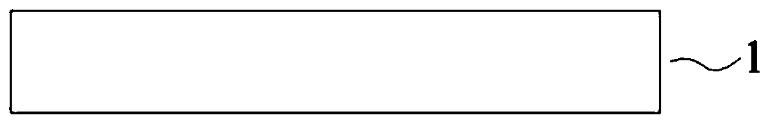
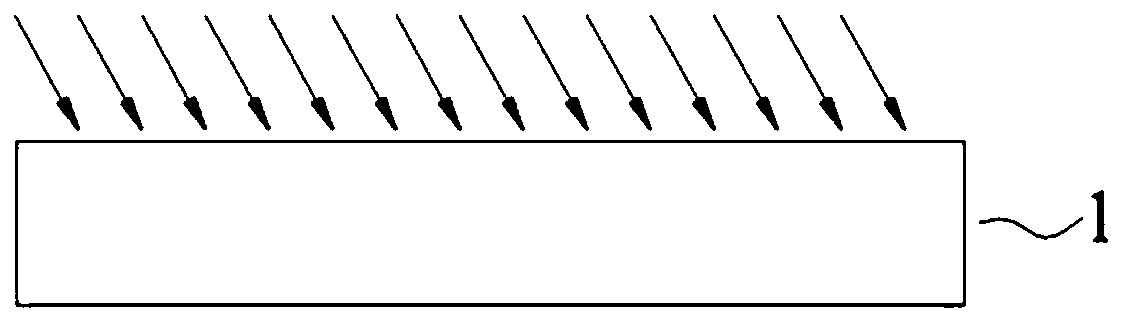
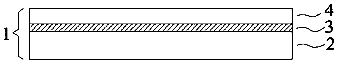
[0060] Such as Figure 1-5 As shown, ion implantation is performed on the upper surface of the n-type conductive silicon carbide semiconductor substrate layer 1, preferably 5 μm or 10 μm; after ion implantation, a layer of ion damage layer 3 is generated under the surface of the semiconductor substrate layer 1, so that the n-type conductive silicon carbide semiconductor The substrate layer 1 is divided into the substrate main body layer 2, the ion damage layer 3 and the silicon carbide film layer 4 located on the upper surface of the ion damage layer 3 from bottom to top; For the n-type silicon carbide epitaxial layer 5 with a low bottom, aluminum ions are implanted on the surface of the epitaxial layer to form p-type conductive points, and nickel is electroplated on the epitaxial layer as a Schottky barrier layer 6 (stress introduction layer). Separate the epitaxial layer and the silicon carbide film layer under the epitaxial layer from the silicon carbide substrate, and use ...

Embodiment 2

[0063] Perform ion implantation on the upper surface of the silicon carbide substrate layer 1, the ion implantation depth is 0.5 μm-20 μm, preferably 5 μm, 10 μm, and 15 μm; after the ion implantation, a layer of ion damage layer 3 is generated under the surface of the silicon carbide substrate layer 1, thereby The n-type conductive silicon carbide semiconductor substrate layer 1 is divided into the substrate main body layer 2, the ion damage layer 3 and the silicon carbide film layer 4 located on the upper surface of the ion damage layer 3 from bottom to top; the ion implantation surface of the silicon carbide film layer 4 Prepare the functional layer (electronic device layer), the electronic device in this embodiment is a semiconductor epitaxial layer 5 grown epitaxially on the upper surface of the silicon carbide substrate 1, or a semiconductor epitaxial layer grown epitaxially on the upper surface of the semiconductor substrate layer 1 5 and the semiconductor electronic dev...


PUM

PropertyMeasurementUnit
thicknessaaaaaaaaaa

Abstract

The invention relates to a manufacturing method of a thin-film electronic device with a vertical structure on a silicon carbide substrate. The method comprises the following steps of (S1) carrying oution implantation on the silicon carbide substrate and dividing the silicon carbide substrate into a substrate main body layer, an ion damage layer and a silicon carbide thin-film layer located on theupper surface of the ion damage layer from bottom to top; (S2) manufacturing an electronic device layer on the silicon carbide thin-film layer; (S3) removing the residual ion damage layer on the surface of the silicon carbide thin-film layer after separation through an ion thinning or plasma etching method; and (S4) manufacturing an electrode on the surface of the separated device. The manufacturing method of the thin-film electronic device with the vertical structure on the silicon carbide substrate mainly aims at solving the problem of resistivity increase caused by the residual ion damagelayer on the surface of the silicon carbide substrate after ion cutting and separation, and the disadvantages that machining of a thin film is not easy and a few of semiconductor materials are not strong in atomic mobility are avoided.

Description

technical field [0001] The invention relates to the field of electronic devices, in particular to a thin-film electronic device with a vertical structure on a silicon carbide substrate and a manufacturing method thereof. Background technique [0002] Silicon carbide is a wide-bandgap semiconductor material. Compared with silicon, the most widely used semiconductor material, it has good thermal conductivity, high operating temperature, high current density, high breakdown electric field strength, high operating frequency, and power consumption under high current. Small and other advantages. However, the high price of silicon carbide substrates compared with other semiconductor materials limits the wide application of silicon carbide materials. At present, electronic devices made of silicon carbide materials are mainly based on silicon carbide substrates with a thickness of 0.43 mm, and the price of the substrate can be as high as 1 / 3 of the device manufacturing cost. If the...

Claims


Application Information

Patent Timeline
Patent Type & Authority Patents(China)
IPC IPC(8): H01L21/02H01L29/872H01L33/32
CPCH01L21/02378H01L21/02428H01L29/872H01L33/32
Inventor 胡兵朱元勋
Owner 朱元勋
Why Eureka
Try Eureka