Femtosecond laser micromachining method and device
A femtosecond laser and micromachining technology, applied in laser welding equipment, metal processing equipment, manufacturing tools, etc., can solve problems affecting processing quality and processing accuracy, recasting layers in processing areas, thermal deformation and cracks, etc., to achieve improved Processing quality and processing accuracy, the effect of avoiding the heat-affected zone
- Summary
- Abstract
- Description
- Claims
- Application Information
AI Technical Summary
Problems solved by technology
Method used
Image
Examples
Embodiment 1
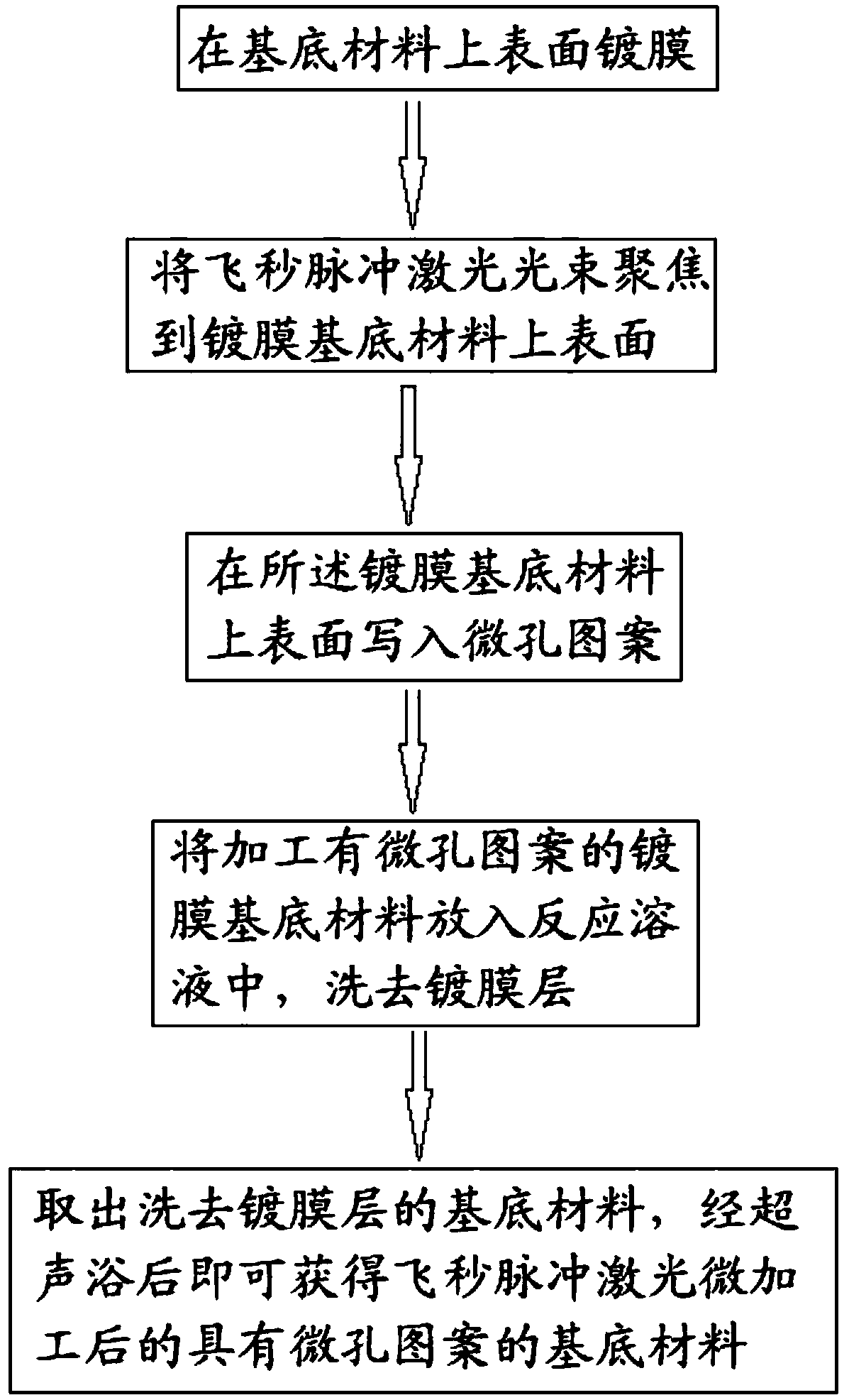
[0032] The embodiment of the present invention provides a femtosecond laser micromachining method, please refer to figure 1 , the method includes:
[0033] Step 10: coating the surface of the base material.
[0034] Specifically, electron beam evaporation is used to coat the surface of the base material to avoid phenomena such as heat-affected zones, recast layers, thermal deformation and cracks during processing.
[0035] Step 20: focusing the femtosecond pulsed laser beam onto the upper surface of the coating base material.
[0036] Specifically, the femtosecond pulsed laser beam is focused on the upper surface of the coated base material to prepare for subsequent micro-hole processing on the upper surface of the coated base material.
[0037] Step 30: Writing a microhole pattern on the upper surface of the coating base material.
[0038] Specifically, the computer controls the femtosecond pulsed laser beam to write the required microhole pattern on the upper surface of t...
Embodiment 2
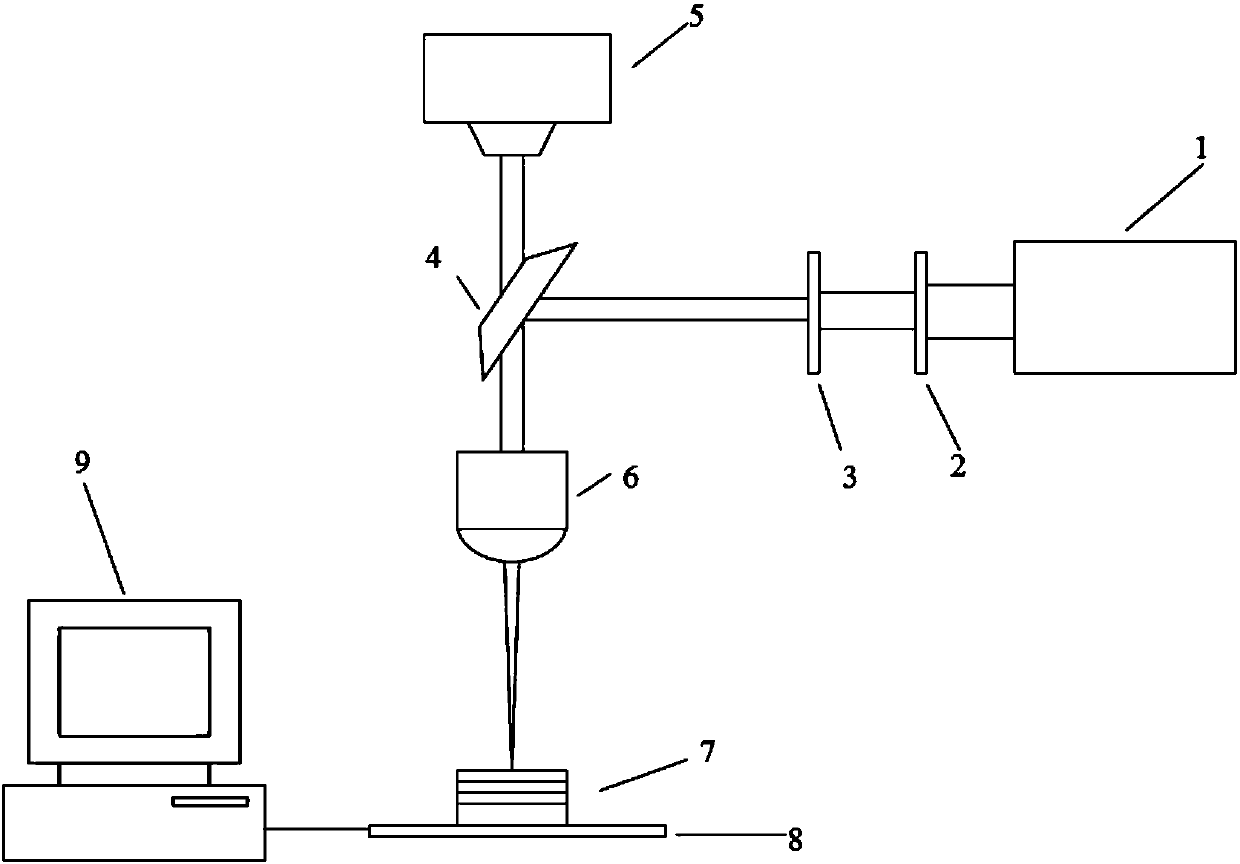
[0051] The embodiment of the present invention provides a femtosecond laser micromachining device, please refer to figure 2 , the device includes:
[0052] femtosecond laser1.
[0053] Specifically, the femtosecond laser 1 emits a femtosecond pulsed laser beam with a wavelength of 800 nm, a pulse width of 45 fs, and a pulse frequency of 1 kHz.
[0054] Mirror 4.
[0055] Specifically, the reflector 4 receives the femtosecond pulsed laser beam emitted by the femtosecond laser 1, and reflects the femtosecond pulsed laser beam to the microscopic objective lens 6, and the reflector 4 plays a role in changing the Technical effects of femtosecond pulsed laser beam paths.
[0056] Microscope objective 6.
[0057] Specifically, the microscopic objective lens 6 receives the femtosecond pulsed laser beam reflected from the mirror 4, and focuses the femtosecond pulsed laser beam.
[0058] Electronically controlled translation stage 8.
[0059] Specifically, the material 7 to be pr...
Embodiment 3
[0069] Embodiments of the present invention provide specific process steps of a femtosecond laser micromachining method, please refer to figure 1 , figure 2 .
[0070] Step 1: Preparation of coating base material.
[0071] A 10-fused silica sample with a size of 10mm×10mm×0.5mm and polished six sides was used as the base material, and copper, aluminum, and silver were used as coating materials, and the coating sequence was silver, copper, and aluminum. Electron beam evaporation technology is used to prepare coating samples in the vacuum chamber of the electron beam evaporation system. The base material was cleaned in an ultrasonic bath in ethanol, acetone and deionized water for 10 minutes, dried with nitrogen, and quickly placed in the vacuum chamber of the electron beam evaporation system, and the film material was put into the corresponding crucible, and then Evacuate the electron beam evaporation system to above 10 -3 Pa, then raise the temperature of the substrate su...
PUM
| Property | Measurement | Unit |
|---|---|---|
| Average power | aaaaa | aaaaa |
| Pulse width | aaaaa | aaaaa |
| Center wavelength | aaaaa | aaaaa |
Abstract
Description
Claims
Application Information
 - R&D
- Intellectual Property
- Life Sciences
- Materials
- Tech Scout
- Unparalleled Data Quality
- Higher Quality Content
- 60% Fewer Hallucinations
Browse by: Latest US Patents, China's latest patents, Technical Efficacy Thesaurus, Application Domain, Technology Topic, Popular Technical Reports.
© 2025 PatSnap. All rights reserved.Legal|Privacy policy|Modern Slavery Act Transparency Statement|Sitemap|About US| Contact US: help@patsnap.com


