Method for corroding indium phosphide single crystal wafer

A technology of indium phosphide single crystal and indium single crystal, which is applied in the field of semiconductors, and can solve the problems of affecting the use effect of the substrate, insufficient removal of the stress layer, and small removal of the surface of the indium phosphide single wafer.

Inactive Publication Date: 2018-02-23
珠海鼎泰芯源晶体有限公司
View PDF5 Cites 1 Cited by
  • Summary
  • Abstract
  • Description
  • Claims
  • Application Information

AI Technical Summary

Problems solved by technology

The disadvantages of this method are: firstly, it takes a long time to cool the etching solution after it is prepared, and the efficiency is low; secondly, the removal amount of the surface of the indium phosphide single wafer is very small, so it is necessary to remove the damage caused by cutting, grinding and other processing processes. Deep surface mechanical damage and insufficient stress layer removal will affect the later use of the substrate

Method used


Image

  • Method for corroding indium phosphide single crystal wafer

Examples


Embodiment Construction

[0025] Embodiments of the present invention will be described below with reference to the accompanying drawings. Those skilled in the art would recognize that the described embodiments can be modified in various ways or combinations thereof without departing from the spirit and scope of the invention. Accordingly, the drawings and description are illustrative in nature and not intended to limit the scope of the claims. Also, in this specification, the drawings are not drawn to scale, and like reference numerals denote like parts.

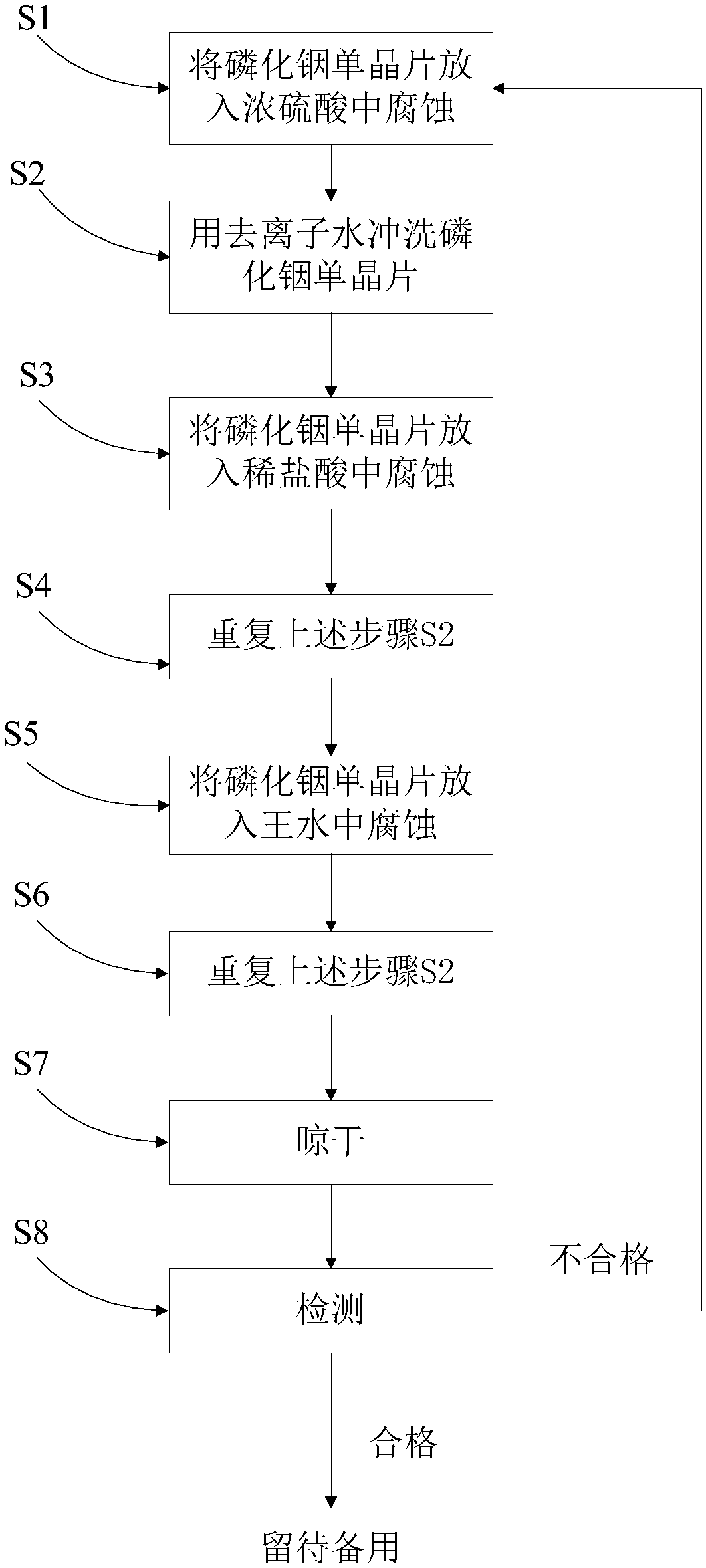
[0026] Combine below figure 1 This embodiment will be described in detail.

[0027] figure 1 It is a schematic flow chart of an etching method for an indium phosphide single wafer according to the present invention, as figure 1 Shown, the etching method of described indium phosphide single wafer comprises the following steps:

[0028] S1 corrodes the indium phosphide single wafer in concentrated sulfuric acid;

[0029] S2 rinses the indium pho...


PUM


Abstract

The invention discloses a method for corroding an indium phosphide single crystal wafer. The method comprises the following steps: S1, corroding an indium phosphide single crystal wafer into concentrated sulfuric acid; S2, irrigating the indium phosphide single crystal wafer with deionized water; S3, corroding the indium phosphide single crystal wafer in diluted hydrochloric acid; S4, repeating the step S2; S5, corroding the indium phosphide single crystal wafer in chloroazotic acid; S6, repeating the step S2; and S7, drying in the air. According to the method, the split and ground indium phosphide single crystal wafer is corroded by adopting an acid corrosion mode, the damage layer and stress layer on the surface of the single crystal wafer can be effectively removed, and a clean single crystal wafer surface can be obtained to meet the requirement for subsequent processing.

Description

technical field [0001] The invention relates to the technical field of semiconductors, in particular to an etching method for an indium phosphide single wafer. Background technique [0002] Indium phosphide single crystal is an important compound semiconductor material with a mothite structure. It has the characteristics of high electronic limit drift speed, good radiation resistance, high thermal conductivity, and high breakdown electric field. Therefore, indium phosphide single crystal material is the preferred substrate material in the preparation of microwave, millimeter wave circuits and high-speed digital integrated circuits. In recent years, the country has invested considerable funds in the development of indium phosphide single wafer substrate materials. Chemical etching is a very important step in the processing of indium phosphide single wafer. Its main function is to remove the mechanical damage caused by cutting, grinding and other processing processes on the ...

Claims


Application Information

Patent Timeline
Patent Type & Authority Applications(China)
IPC IPC(8): C30B33/10C30B29/40
CPCC30B29/40C30B33/10
Inventor 刘京明杨凤云王凤华段满龙
Owner 珠海鼎泰芯源晶体有限公司
Why Eureka
Try Eureka