A high-precision positioning method for LED chip array arrangement
A LED chip and array arrangement technology, which is applied in the manufacture of semiconductor devices, electrical components, semiconductor/solid-state devices, etc., can solve the problems of chip integration failure, high investment cost, and affecting the yield rate of chip integration, so as to ensure the uniformity of color temperature performance, increase shipment rate, and ensure consistency
- Summary
- Abstract
- Description
- Claims
- Application Information
AI Technical Summary
Problems solved by technology
Method used
Image
Examples
Embodiment 1
[0045]The existing ordinary chip placement equipment has a low accuracy of only ±30um in chip positioning; while high-precision chip placement equipment can improve the accuracy to ±10um, but the price of high-precision chip placement equipment is as high as nearly one million yuan. Replacement of high-precision chip placement equipment Equipment saving investment is too high. In order to solve the above problems, this embodiment provides a high-precision positioning method for LED chip arrays, which can improve the positioning accuracy of the chips to below ±10um by using existing common chip arrangement equipment.
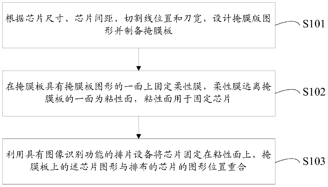
[0046] figure 1 A process flow chart of the high-precision positioning method of the LED chip array in this embodiment is given. See figure 1 , the positioning method, including:
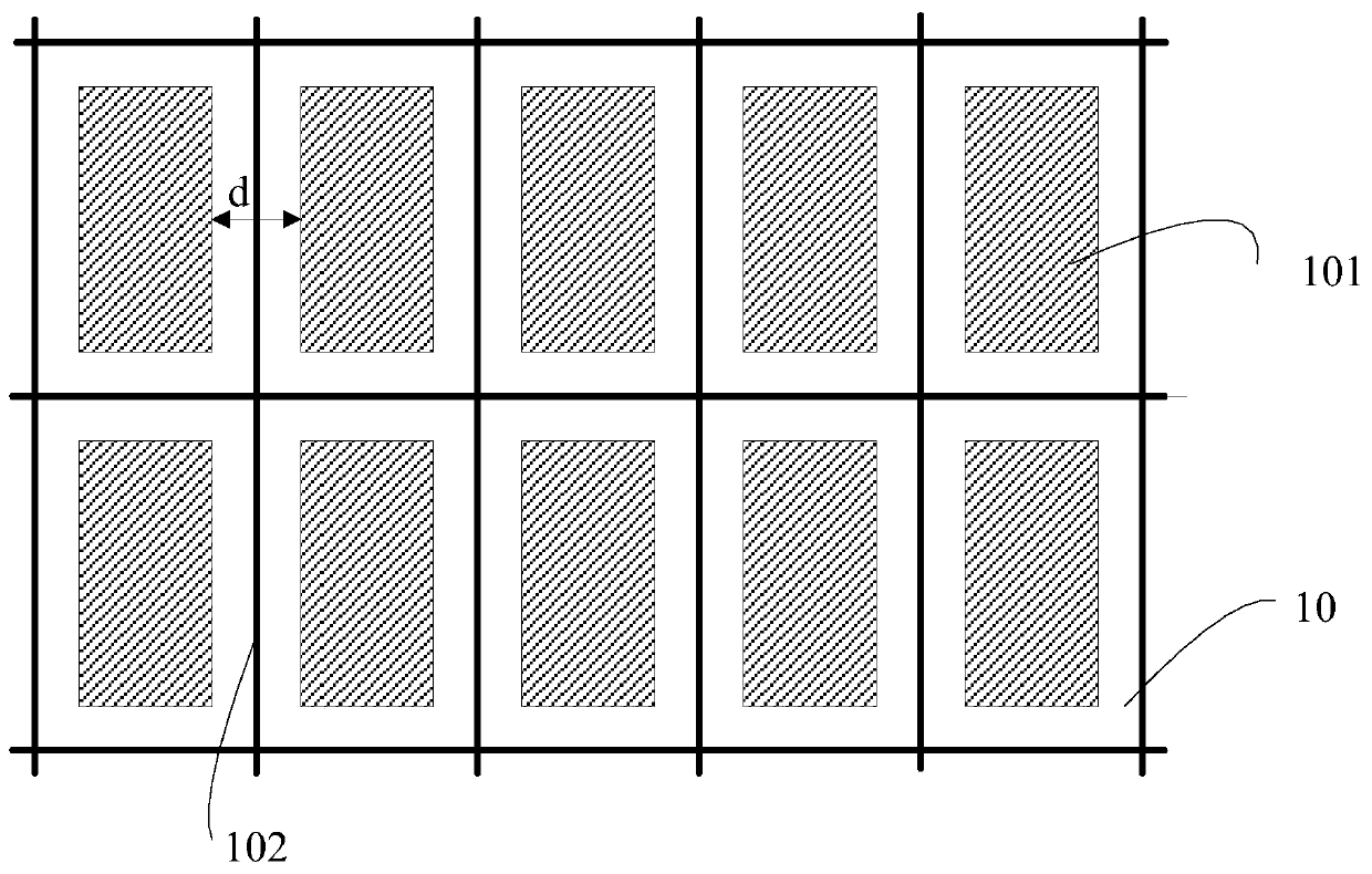
[0047] Step S101: figure 2 A top view schematic diagram of step S101 in this embodiment is given, and a mask pattern is designed and a mask plate is made according to the chip siz...
Embodiment 2
[0056] Figure 6 A process flow chart of the high-precision positioning method of the LED chip array in this embodiment is given. See Figure 6 , the positioning method, including:
[0057] Step S201: Figure 7 A top view schematic diagram of step S201 in this embodiment is given, and a mask pattern is designed and a mask plate is made according to the chip size, the chip spacing d, the position of the cutting line 102 and the knife width.
[0058] Figure 8 A cross-sectional schematic diagram of step S201 in this embodiment is given, please refer to Figure 7 and Figure 8 , forming a light blocking layer 10 on the glass substrate 20, using photolithography technology to etch the light blocking layer 10 to form a mask pattern, the mask pattern includes a plurality of chip patterns 101 arranged in an array, and the chip pattern 101 The light blocking layer 10 is etched away.
[0059] Need to explain is, Figure 7 There are 10 chip patterns 101 in the mask plate given i...
Embodiment 3
[0066] figure 1 The process flow chart of the high-precision positioning method of the LED chip array in this embodiment is given, please refer to Figure 11 , the present embodiment provides a high-precision positioning method for an LED chip array, including:
[0067] Step S301: Design a mask pattern and make a mask plate according to the chip size, chip pitch, dicing line position and knife width. The mask pattern includes a plurality of chip patterns arranged in an array.
[0068] Step S302: Fix the flexible film on the side of the mask plate having the pattern of the mask plate, the side of the flexible film 2 away from the mask plate is an adhesive surface, and the adhesive surface is used to fix the chip.
[0069] It should be noted that the flexible film in the present invention is a transparent film with a temperature resistance greater than 150°C. The flexible film can be a double-sided adhesive film or a single-sided adhesive film. If the flexible film is a double...
PUM
 Abstract
Description
Claims
Application Information


