Plasmon-structured substrate and preparation method and application thereof

A technology of plasmons and substrates, which is applied in the field of substrates of perovskite-based optoelectronic devices, can solve problems affecting device stability and changing material structures, and achieve strong structural stability, convenient preparation, and high stability Effect

Active Publication Date: 2018-02-23
PEKING UNIV
View PDF6 Cites 11 Cited by
  • Summary
  • Abstract
  • Description
  • Claims
  • Application Information

AI Technical Summary

Problems solved by technology

[0004] It is a research hotspot in the field of solar cells to enhance absorption by chemically doping nano-metal particles into perovskite

Method used


Image

  • Plasmon-structured substrate and preparation method and application thereof
  • Plasmon-structured substrate and preparation method and application thereof
  • Plasmon-structured substrate and preparation method and application thereof

Examples


preparation example Construction

[0051] The preparation method of the perovskite photodetector based on the plasmonic structure substrate is further provided below, including the following steps:

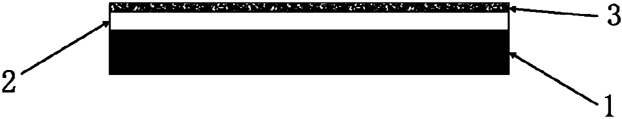
[0052] Step 1, the SiO 2 / Si substrate 1 is ultrasonically cleaned with an organic solvent, and ultrasonically cleaned in the order of acetone (10-15min)→ethanol (10-20min)→deionized water (20-30min), and finally removes the residues on the substrate with a nitrogen gun. Blow dry with ion water to get clean SiO 2 / Si substrate.

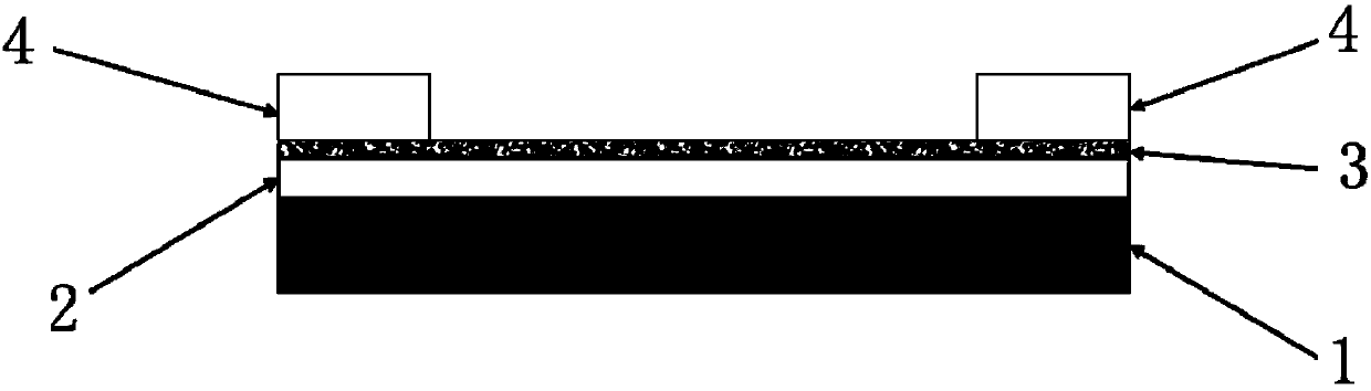
[0053] Step two, such as figure 1 As shown, the SiO obtained in the previous step 2 The Si surface of the / Si substrate 1 is plated with gold as the reflective layer 2 by electron beam evaporation coating method, and then coated with SiO by thermal evaporation coating method. 2 as insulating layer 3. In order to obtain a better film quality, the vacuum degree of the electron beam evaporation coating instrument and the thermal evaporation coating instrument should be pumped to 10 -8 ...

Embodiment 1

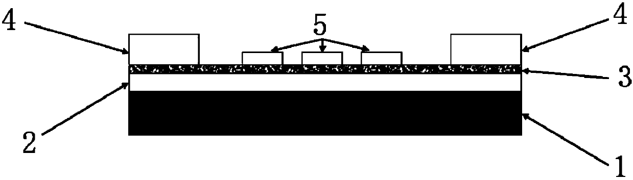
[0059] SEM image of a perovskite photodetector based on a plasmonic substrate Figure 5 shown, bottom-up including SiO 2 / Si substrate 1, gold film reflective layer 2, SiO 2 Insulating layer 3, positive and negative electrodes 4, gold rectangular array 5 and hole transport layer 6, CH 3 NH 3 PB 3 Absorbent layer7. Among them, the gold film reflective layer 2 is deposited on SiO by electron beam evaporation. 2 / Si substrate 1, SiO coated by thermal evaporation 2 The insulating layer 3 is on the gold film reflective layer 2, and the positive and negative electrodes 4 produced by electron beam exposure are on the SiO 2 On the insulating layer 3, 3nmTi / 50nm Au is obtained by electron beam evaporation. Gold rectangular array 5 in SiO 2 On the insulating layer 3 and between the two positive and negative electrodes 4, the material is gold, the height is 30nm, the side length is 250nm, the period is 350nm, and the array size is 30μm×30μm. (Under this radius and period, the fi...


PUM

PropertyMeasurementUnit
Thicknessaaaaaaaaaa
Thicknessaaaaaaaaaa
Thicknessaaaaaaaaaa

Abstract

The invention discloses a plasmon-structured substrate and a preparation method and an application thereof. The plasmon-structured substrate comprises a substrate, a reflective layer, an insulating layer, a metal nano-structure array and a positive electrode and a negative electrode; a perovskite device enhanced substrate is prepared based on a plasmon field enhancement principle initially; and byvirtue of a physical method, absorption limited expansion of the perovskite material in an infrared light waveband and absorption enhancement in the whole absorption region are realized, so that negative effects caused by chemical doping of a perovskite layer is avoided.

Description

technical field [0001] The invention relates to a substrate for perovskite-based optoelectronic devices, specifically an enhanced absorption limit substrate for perovskite photodetectors and perovskite solar cells, which can enhance the overall absorption efficiency of perovskite materials and Extend its absorption area in the near-infrared range. Background technique [0002] Perovskite (perovskite) material refers to the material with CaTiO 3 A class of organic-inorganic hybrid materials of the same crystal structure, belonging to semiconductors. Its chemical formula is AMX 3 , where A is generally an organic cation CH 3 NH 3+ and HN=CH(NH 3 ) + etc., M is a divalent metal ion Pb 2+ or Sn 2+ etc. X is a halogen ion such as Cl, Br or I. In recent years, perovskite materials have been widely used in solar cells, photodetectors and other fields due to their excellent properties such as high electron mobility, high carrier density, wide-band absorption, stable structu...

Claims


Application Information

Patent Timeline
IPC IPC(8): H01L51/44H01L51/48
CPCH10K71/00H10K30/87Y02E10/549Y02P70/50
Inventor 方哲宇杜博文朱星
Owner PEKING UNIV
Why Eureka
Try Eureka