A kind of semiconductor device and its manufacturing method, electronic device

A manufacturing method and semiconductor technology, applied in semiconductor devices, electric solid state devices, circuits, etc., can solve the problems of increased electron traps, large leakage current, limited key size, etc., to reduce leakage current, improve the programming window, and increase the key The effect of size

Active Publication Date: 2020-11-10
SEMICON MFG INT (SHANGHAI) CORP +1
View PDF4 Cites 0 Cited by
  • Summary
  • Abstract
  • Description
  • Claims
  • Application Information

AI Technical Summary

Problems solved by technology

[0003] As the critical dimensions of NAND flash memory cells shrink below 20nm, the critical dimensions of the floating gate (FG) are getting smaller and smaller. The thickness of (IPD) cannot be reduced all the time, for example, it must maintain a thickness of about 10nm. Under the influence of these two factors, such as figure 1 As shown by the dotted line area, the critical dimension of the top of the floating gate is very limited (in other words, the top of the floating gate forms a tip), which leads to a large leakage current in the IPD during programming, which in turn leads to a greatly reduced maximum threshold voltage in the programming window. Small, and the electronic trap (trap) in the IPD increases, which will affect the device performance, such as programming ability, endurance, data retention ability, etc.

Method used


Image

  • A kind of semiconductor device and its manufacturing method, electronic device
  • A kind of semiconductor device and its manufacturing method, electronic device
  • A kind of semiconductor device and its manufacturing method, electronic device

Examples


Embodiment 1

[0043] The following will refer to Figure 3A ~ Figure 3G as well as Figure 4 A method for fabricating a semiconductor device according to an embodiment of the present invention will be described in detail.

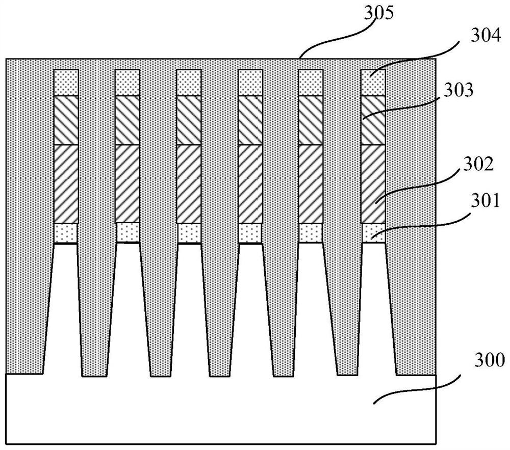
[0044] First, if Figure 3A As shown, a semiconductor substrate 300 is provided, a floating gate array 302 is formed on the semiconductor substrate 300, a trench forming an isolation structure is formed in the semiconductor substrate 300, and between the floating gate arrays 302 The gaps and the trenches are filled with isolation material 305 .

[0045] Wherein, the semiconductor substrate 300 can be at least one of the materials mentioned below: Si, Ge, SiGe, SiC, SiGeC, InAs, GaAs, InP or other III / V compound semiconductors, and also includes multiple semiconductors composed of these semiconductors. The layer structure or the like may be silicon-on-insulator (SOI), silicon-on-insulator (SSOI), silicon-germanium-on-insulator (S-SiGeOI), silicon-germanium-on-insulator...

Embodiment 2

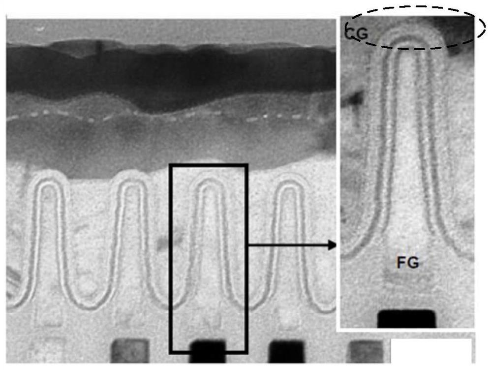
[0077] The present invention also provides a semiconductor device fabricated by the above method, such as Figure 5 As shown, the semiconductor device includes: a semiconductor substrate 500, an isolation structure 501 is formed in the semiconductor substrate 500, a gate oxide layer 502 is formed on the semiconductor substrate between the isolation structures, and between the gate oxide layer 502 A floating gate 503 is formed on it, a current blocking layer 504 is formed on the top of the floating gate 503 , and a gate dielectric layer 505 is formed on the sidewall of the floating gate 503 and the top of the current blocking layer 504 .

[0078] Wherein the semiconductor substrate 500 can be at least one of the materials mentioned below: Si, Ge, SiGe, SiC, SiGeC, InAs, GaAs, InP or other III / V compound semiconductors, and also includes multilayers composed of these semiconductors The structure or the like may be silicon-on-insulator (SOI), silicon-on-insulator (SSOI), silicon-...

Embodiment 3

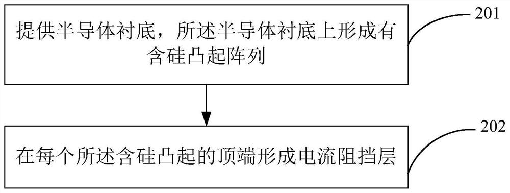
[0085] Still another embodiment of the present invention provides an electronic device, including a semiconductor device and an electronic component connected to the semiconductor device. Wherein, the semiconductor device includes: a semiconductor substrate, an array of silicon-containing protrusions is formed on the semiconductor substrate, and a current blocking layer is formed on the top of each silicon-containing protrusion.

[0086] The semiconductor substrate can be at least one of the materials mentioned below: Si, Ge, SiGe, SiC, SiGeC, InAs, GaAs, InP or other III / V compound semiconductors, including multilayer structures composed of these semiconductors etc. or silicon-on-insulator (SOI), silicon-on-insulator (SSOI), silicon-germanium-on-insulator (S-SiGeOI), silicon-germanium-on-insulator (SiGeOI), and germanium-on-insulator (GeOI). Devices, such as NMOS and / or PMOS, can be formed on the semiconductor substrate. Similarly, a conductive member may also be formed in t...


PUM


Abstract

The present invention provides a semiconductor device, a manufacturing method thereof, and an electronic device. The manufacturing method includes: providing a semiconductor substrate on which an array of silicon-containing protrusions is formed; A current blocking layer is formed. The manufacturing method can form a current blocking layer on the top of the silicon-containing protrusion, thereby avoiding the formation of a conductive tip on the top of the silicon-containing protrusion, thereby relatively increasing the critical dimension of the conductive part at the top of the silicon-containing protrusion, reducing leakage current, and improving the performance of the silicon-containing protrusion. Device performance such as programming window, endurance, and data retention. The semiconductor device and electronic device have high performance.

Description

technical field [0001] The present invention relates to the technical field of semiconductors, in particular to a semiconductor device, a manufacturing method thereof, and an electronic device. Background technique [0002] With the development of semiconductor manufacturing technology, flash memory (flash memory) with faster access speed has been developed in terms of storage devices. Flash memory has the characteristics that information can be stored, read, and erased multiple times, and the stored information will not disappear after power failure. Therefore, flash memory has become a popular choice for personal computers and electronic devices. A widely used type of non-volatile memory. However, NAND (NAND gate) fast memory is widely used in fields with high read / write requirements due to its large storage capacity and relatively high performance. Recently, the capacity of NAND flash memory chips has reached 2GB, and the size is rapidly increasing. Solid state drives ...

Claims


Application Information

Patent Timeline
Patent Type & Authority Patents(China)
IPC IPC(8): H01L27/11517
CPCH10B41/00
Inventor 陈卓凡张翼英
Owner SEMICON MFG INT (SHANGHAI) CORP
Why Eureka
Try Eureka