Junction temperature test method of AlGaN/GaN high electron mobility transistor

A technology with high electron mobility and transistors, which is applied in semiconductor/solid-state device testing/measurement, circuits, electrical components, etc. It can solve problems such as large error in measurement results, failure to meet measurement requirements, and underestimation of device junction temperature. Simplicity, increased accuracy, and easy-to-achieve results

Active Publication Date: 2018-03-23
XIDIAN UNIV
View PDF7 Cites 11 Cited by
  • Summary
  • Abstract
  • Description
  • Claims
  • Application Information

AI Technical Summary

Problems solved by technology

N.Killat et al. used the infrared method to extract the junction temperature of AlGaN/GaN HEMT devices and compared them with the Raman test results. They found that the infrared test results were far lower than the actual junction temperature of the device. See N.Killat, M.Kuball ,T.–M.Chou,etc.Temperature Assessment of AlGaN/GaN HEMTs:A Comparative study by Raman,Electrical and IR Thermography.IEEE Conference Publications,2010,528-531, the spatial resolution of the infrared method is only 2.5μm, However, the gate length of HEMT devices is generally less than 1 μm, and the source-drain distance is only a few μm. The junction temperature of the device generally appears at the edge of the gate near the drain. Therefore, the resolution of the infrared method is far from meeting the measurement requirements, resulting in measurement Th

Method used


Image

  • Junction temperature test method of AlGaN/GaN high electron mobility transistor

Examples


Embodiment 1

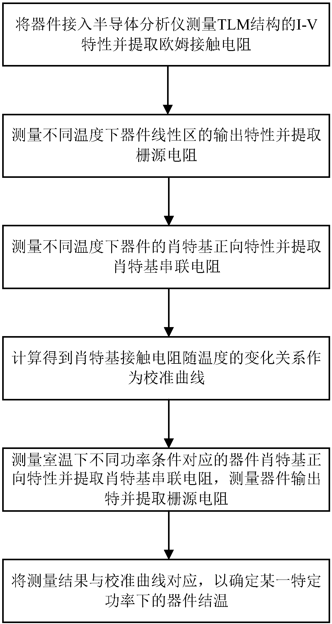
[0018] Embodiment 1: Testing the junction temperature of an AlGaN / GaN HEMT device on a sapphire substrate.

[0019] Step 1, measure the ohmic contact resistance R of the transmission line model TLM structure C .

[0020] 1a) Place the tested AlGaN / GaN high electron mobility transistor HEMT device on the sapphire substrate on the probe station, apply a voltage to the transmission line model TLM structure through the semiconductor parameter analyzer, and set the voltage range from -0.5V to 0.5V ;

[0021] 1b) Test the current-voltage I-V characteristics of the TLM structure of the transmission line model, and extract the ohmic contact resistance R of the device under test C ;

[0022] Step 2, measure the on-resistance R of the AlGaN / GaN high electron mobility transistor HEMT device ON0 .

[0023] 2a) Place the tested AlGaN / GaN high electron mobility transistor HEMT device on the probe station, the source is grounded, and the gate voltage is set to V GS and drain voltage V ...

Embodiment 2

[0043] Embodiment 2: Testing the junction temperature of an AlGaN / GaN HEMT device on a silicon carbide substrate.

[0044] Step 1, measure the ohmic contact resistance R of the transmission line model TLM structure C .

[0045] Step 1 of this example is the same as Step 1 of Embodiment 1.

[0046] Step 2, measure the on-resistance R of the AlGaN / GaN high electron mobility transistor HEMT device ON0 .

[0047] 2a) Place the tested AlGaN / GaN high electron mobility transistor HEMT device on the probe station, the source is grounded, and the gate voltage is set to V GS and drain voltage V DS The pulse width is 500ns, the pulse period is 1ms, and the gate static bias point is V GSQ with the source statically biased at the point V DSQ is 0V, the drain voltage V DS From 0V to 12V, the gate voltage V is applied to it through the semiconductor parameter analyzer GS and drain voltage V DS ;

[0048] 2b) Adjust the temperature controller to apply different external temperatures...

Embodiment 3

[0068] Embodiment 3: Junction temperature test of AlGaN / GaN HEMT device on silicon substrate

[0069] Step 1, measure the ohmic contact resistance R of the transmission line model TLM structure C .

[0070] This step is the same as Step 1 in Example 1.

[0071] Step 2, measure the on-resistance R of the AlGaN / GaN high electron mobility transistor HEMT device ON0 .

[0072]2a) Place the tested AlGaN / GaN high electron mobility transistor HEMT device on the probe station, the source is grounded, and the gate voltage is set to V GS and drain voltage V DS The pulse width is 500ns, the pulse period is 1ms, and the gate static bias point is V GSQ with the source statically biased at the point V DSQ is 0V, the drain voltage V DS From 0V to 12V, the gate voltage V is applied to it through the semiconductor parameter analyzer GS and drain voltage V DS ;

[0073] 2b) Adjust the temperature controller to apply different external temperatures to the device, measure the output cha...


PUM


Abstract

The invention discloses a junction temperature test method of an AlGaN/GaN high electron mobility transistor and mainly solves a problem of the relatively low measured junction temperature existing ina method in the prior art. The method comprises steps that a pulse test method is utilized to test schottky positive characteristics of a device, the change relationship between gate source resistance RS0 and Schottky series resistance RT0 along with the temperature is extracted, and the change relationship of Schottky contact resistance RB0 along with the temperature is acquired as a calibrationcurve through combining the above two factors; secondly, a bias point is selected under the room temperature condition, the pulse test method is utilized to test the Schottky forward characteristicsof the device, Schottky series resistance RT is further extracted, output characteristics of a detected device are measured, gate source resistance RS is extracted, the change relationship of Schottkycontact resistance RB under different powers is acquired, through comparing with a calibration curve, the device junction temperature is extracted. The method is advantaged in that accuracy of the junction temperature test is improved, the measurement error is reduced, and the method can be used for measurement and analysis of high electron mobility transistor devices.

Description

technical field [0001] The invention belongs to the technical field of semiconductor devices, in particular to a junction temperature testing method of an AlGaN / GaN high electron mobility transistor HEMT, which can be used for device measurement and analysis. technical background [0002] AlGaN / GaN high electron mobility transistor HEMT has a very broad development prospect in the application of high temperature and microwave high power, and has attracted extensive attention in the past few decades. This is mainly based on the excellent characteristics of GaN materials such as wide bandgap, high breakdown field strength, and high saturation electron drift velocity. Although AlGaN / GaN HEMT has great potential in the future, the thermal reliability of the device is still one of the bottlenecks restricting its development. In high-temperature applications, the significant self-heating effect of AlGaN / GaN HEMT devices will increase the junction temperature of the device and deg...

Claims


Application Information

Patent Timeline
IPC IPC(8): H01L21/66
CPCH01L22/12
Inventor 马晓华武玫闵丹杨凌郝跃
Owner XIDIAN UNIV
Why Eureka
Try Eureka