Highlight flip LED chip having insulating protection structure and manufacturing method thereof

An LED chip and protection structure technology, applied in electrical components, circuits, semiconductor devices, etc., can solve the problems of low brightness, low chip IR yield, and reduced chip packaging yield, so as to improve packaging yield and improve IR quality. rate, the effect of reducing the ability to migrate

Pending Publication Date: 2018-03-30
FOSHAN NATIONSTAR SEMICON
View PDF10 Cites 16 Cited by
  • Summary
  • Abstract
  • Description
  • Claims
  • Application Information

AI Technical Summary

Problems solved by technology

However, Ag easily migrates to the MQW layer (active layer) under the action of the electric field formed by the P-GaN layer and the N-GaN layer, resulting in low IR yield of the chip; and Ag generally does not deposit on the MQW layer, resulting in side The light emitted by the edge MQW layer cannot be received and the brightness is low
In addition, the DBR layer is brittle and hard, and it is easy to cause cracks in the DBR layer when the chip is cut, thereby reducing the chip packaging yield.

Method used


Image

  • Highlight flip LED chip having insulating protection structure and manufacturing method thereof
  • Highlight flip LED chip having insulating protection structure and manufacturing method thereof
  • Highlight flip LED chip having insulating protection structure and manufacturing method thereof

Examples


Embodiment Construction

[0036] In order to make the object, technical solution and advantages of the present invention clearer, the present invention will be further described in detail below in conjunction with the accompanying drawings.

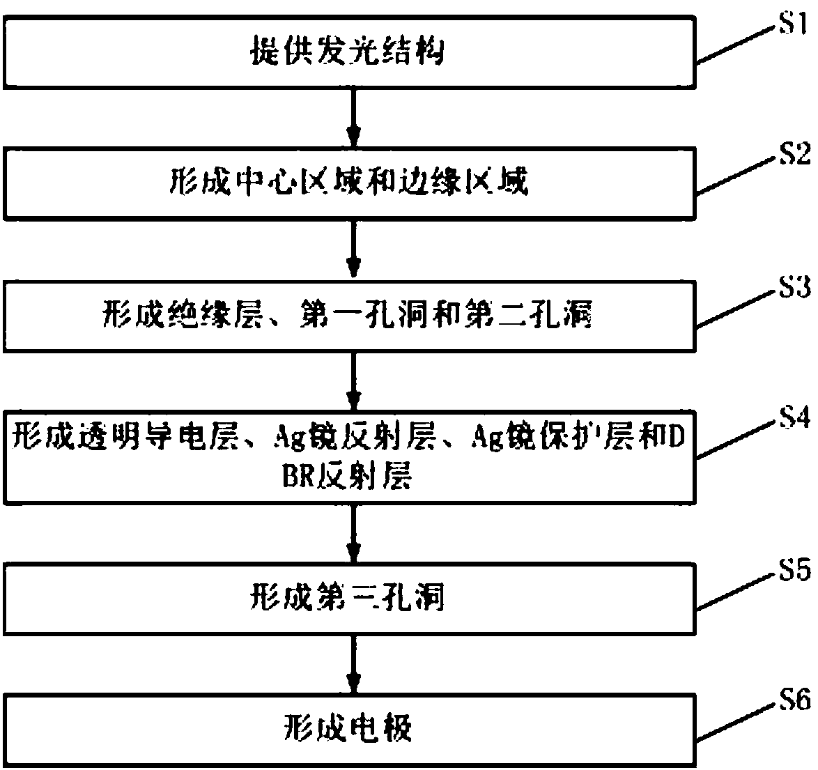
[0037] see figure 1 , figure 1 It is a flowchart of a method for manufacturing a high-brightness flip-chip LED chip with an insulating layer protection structure according to the present invention, wherein the method for manufacturing a high-brightness flip-chip LED chip with an insulation layer protection structure includes the following steps :

[0038] S1: providing a light-emitting structure;

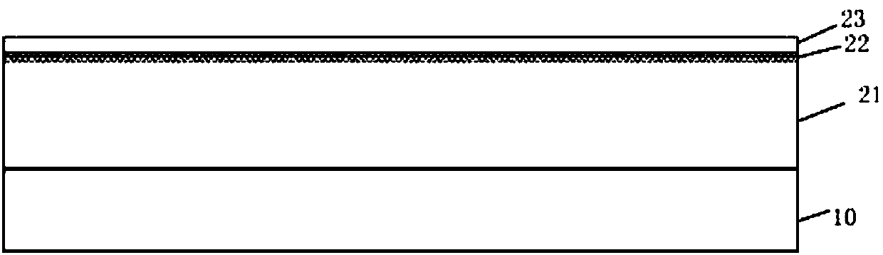
[0039] see Figure 2a , providing a light-emitting structure, the light-emitting structure includes a substrate 10 and an epitaxial layer 20, and the epitaxial layer 20 includes a first semiconductor layer 21, an active layer 22, and a second semiconductor layer 23 sequentially arranged on the surface of the substrate 10 .

[0040] The material of the substrate may...


PUM


Abstract

The invention discloses a manufacturing method of a highlight flip LED chip having an insulating layer protection structure. The manufacturing method comprises the steps that a luminous structure is provided; the luminous structure is etched; an insulating layer is deposited on the surface of the luminous structure; the insulating layer is etched so that a first hole and a second hole are formed;and a transparent conductive layer, an Ag mirror reflection layer, an Ag mirror protection layer and a DBR reflection layer are formed on the surface of the insulating layer and in the first hole andthe second hole. The insulating layer is formed on the surface or the side edge of the first semiconductor layer, the active layer and the second semiconductor layer so that the insulating layer is enabled to cover the bare part of the luminous structure, the Ag can be prevented from migrating to the bare part of the active layer under the effect of the electric field formed by the first semiconductor layer and the second semiconductor layer and the IR yield rate of the chip can be enhanced. Furthermore, the Ag mirror reflection layer covering the insulating layer can effectively reflect out the light emitted by the side edge of the luminous structure so as to enhance the luminous efficiency of the chip.

Description

technical field [0001] The invention relates to the technical field of light-emitting diodes, in particular to a high-brightness flip-chip LED chip with an insulating layer protection structure and a manufacturing method thereof. Background technique [0002] LED (Light Emitting Diode, Light Emitting Diode) is a semiconductor device that uses carrier recombination to release energy to form light. LED chips have low power consumption, pure chromaticity, long life, small size, fast response time, energy saving and environmental protection, etc. Many advantages. [0003] Traditional LED chips are generally sapphire substrates, which have poor heat dissipation performance, prone to leakage, serious light decay, and high voltage, which seriously affect the reliability of LED chips. [0004] Compared with traditional LED chips, flip-chip LED chips have the advantages of high luminous efficiency, uniform current distribution, good heat dissipation, reduced voltage, and high effici...

Claims


Application Information

Patent Timeline
Patent Type & Authority Applications(China)
IPC IPC(8): H01L33/46H01L33/20
CPCH01L33/005H01L33/20H01L33/46
Inventor 范凯平徐亮
Owner FOSHAN NATIONSTAR SEMICON
Why Eureka
Try Eureka