
Substrate structure and its manufacturing method

A technology of substrate and manufacturing method, applied in the field of substrate structure with metal layer and its manufacturing method, can solve the problems of easy delamination, size reduction, difficult roughening process, etc., and achieve the effect of avoiding delamination and improving bonding

Active Publication Date: 2021-08-13
PHOENIX PIONEER TECH
View PDF5 Cites 0 Cited by
  • Summary
  • Abstract
  • Description
  • Claims
  • Application Information

AI Technical Summary

Problems solved by technology

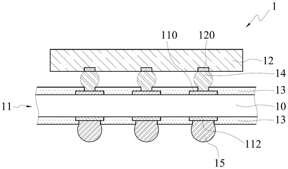
[0004] However, in the packaging substrate 11, the wiring layers 110, 112 are made of different materials from the insulation protection layer 13, and the materials of the dielectric layer 10 and the insulation protection layer 13 are also different, so the manufacturing of the semiconductor package 1 When a temperature cycle (temperature cycle) or stress change is performed during the process, such as when passing through a reflow furnace, or undergoing a process or test such as dropping, the circuit layer 110, 112 and the insulating protection layer 13 or the dielectric layer 10 and the insulating protection layer The areas where heterogeneous materials are combined between layers 13 are easily separated from each other due to Coefficient of thermal expansion (CTE) mismatch, stress concentration, or poor bonding, that is, delamination occurs. The problems caused by these solder bumps 14 and solder balls 15 cannot be effectively electrically connected to the semiconductor chip 12 and the packaging substrate 11, or the product cannot pass the reliability test, resulting in a poor yield rate of the product
[0005] Also, if Figure 1B As shown, although a roughened structure 110a can be formed on the surface of the wiring layer 110, the Ra value of the roughening degree is about 0.1 to 0.5 microns to increase the bonding between the wiring layer 110 and the insulating protection layer 13, but the wiring The bonding surface between the layer 110 and the insulating protection layer 13 still presents a flat surface, causing the distribution direction of the stress to extend continuously along the bonding surface between the circuit layer 110 and the insulating protection layer 13 (such as Figure 1B The arrow direction A shown, that is, the horizontal direction relative to the surface of the dielectric layer 10), so it is still easy to produce delamination
[0006] In addition, with the packaging requirements of miniaturization of semiconductor packages, the size of the circuit layer 110 is also reduced, making it difficult to perform the roughening process.
What's more, even the roughening process cannot effectively prevent the delamination between the circuit layers 110, 112 and the insulating protection layer 13 or between the dielectric layer 10 and the insulating protection layer 13

Method used


Image

  • Substrate structure and its manufacturing method
  • Substrate structure and its manufacturing method
  • Substrate structure and its manufacturing method

Examples


Embodiment Construction

[0049] The implementation manners of the present disclosure are described below through specific specific examples, and those skilled in the art can easily understand other advantages and technical effects of the present disclosure from the content disclosed in this specification.

[0050] It should be noted that the structures, proportions, sizes, etc. shown in the accompanying drawings of this specification are only used to match the content disclosed in the specification for the understanding and reading of those familiar with this technology, and are not used to limit the implementation of the present disclosure. Therefore, it has no technical substantive meaning. Any modification of structure, change of proportional relationship or adjustment of size shall still fall within the scope of The technical content disclosed in this disclosure must be within the scope covered. At the same time, terms such as "above", "first", "second" and "one" quoted in this specification are o...


PUM


Abstract

A substrate structure and its manufacturing method include: a dielectric layer, a metal layer formed on the dielectric layer and having a protrusion, and a protective layer formed on the dielectric layer, the metal layer and the protrusion, and The bonding area and fastening effect between the metal layer and the protection layer are increased by the protrusion, and delamination between the metal layer and the protection layer is avoided.

Description

technical field [0001] The disclosure relates to a substrate structure, in particular to a substrate structure with a metal layer and a manufacturing method thereof. Background technique [0002] With the vigorous development of the electronic industry and the evolution of packaging technology, the size or volume of the semiconductor package is also continuously reduced, and the purpose of making the semiconductor package light, thin and small. The substrates of semiconductor packages currently used in electronic products, such as mobile phone chip carrier boards, lens module circuit boards or coil boards, etc., need to make a large copper area on the surface to achieve the technical effect of heat dissipation or noise reduction, and need Make an insulating protective layer to isolate the circuit and prevent the circuit from contacting other components. [0003] Figure 1A It is a schematic cross-sectional view of a semiconductor package 1 in the prior art. As shown in FIG...

Claims


Application Information

Patent Timeline
Patent Type & Authority Patents(China)
IPC IPC(8): H01L23/495H01L21/60
CPCH01L23/4952H01L24/94H01L2224/16225H01L2924/15311
Inventor 胡文宏
Owner PHOENIX PIONEER TECH
Learn More