Novel silicon carbide (SiC) small-angle tilting table terminal structure and preparation method thereof

A technology of terminal structure and mesa structure, applied in electrical components, circuits, semiconductor devices, etc., can solve the problems of uniform photoresist reflow, limited blocking ability of photoresist mask, difficult terminal structure, etc.

Pending Publication Date: 2018-04-13
INST OF ELECTRONICS ENG CHINA ACAD OF ENG PHYSICS
View PDF0 Cites 9 Cited by
  • Summary
  • Abstract
  • Description
  • Claims
  • Application Information

AI Technical Summary

Problems solved by technology

[0007] Although there have been no related reports on SiC GTO devices using a truly ideal negative-tilt terminal structure at home and abroad, there are some reports on the inclined mesa etching of SiC materials in the technical scheme of SiC avalanche photodetectors (APDs). Photoresist reflow method
However, it is a huge challenge to successfully apply some experience in the field of detectors to the terminal design of GTO power devices.
The first is the problem of whether the photoresist can be uniformly reflowed due to the huge difference in device size. At present, the typical device size of SiC APD is hundreds of microns, while the typical size of GTO ...

Method used


Image

  • Novel silicon carbide (SiC) small-angle tilting table terminal structure and preparation method thereof
  • Novel silicon carbide (SiC) small-angle tilting table terminal structure and preparation method thereof
  • Novel silicon carbide (SiC) small-angle tilting table terminal structure and preparation method thereof

Examples


Embodiment 1

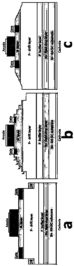
[0028] A new type of small-angle inclined mesa terminal applied to silicon carbide GTO devices. The epitaxial structure of the SiC sample material is a typical P+ / N / P- / P / N+ structure in GTO devices from top to bottom, and the epitaxial layers are in order P+ contact layer (thickness 2μm, doping concentration 1×10 19 cm -3 ), N base layer (thickness 2μm, doping concentration 2×10 17 cm -3 ), P-drift layer (thickness 60μm, doping concentration 2×10 14 cm -3 ), P buffer layer (thickness 2μm, doping concentration 2×10 17 cm -3 ), N+ field stop layer (thickness 1μm, doping concentration 5×10 18 cm -3 ), the bottom is the 4H-SiC intrinsic substrate of N+. The device mesa of the GTO device is a rounded rectangle of 5mm*2.5mm.

[0029] like Figure 5 As shown, it is a schematic diagram of the terminal structure of the silicon carbide GTO device. The terminal structure is prepared on the N+ type SiC intrinsic substrate 101. From the bottom to the top of the conductive N+ type...

Embodiment 2

[0032] A new type of small-angle inclined mesa terminal applied to silicon carbide PiN devices. The epitaxial structure of the SiC sample material is a P+ / N- / N+ structure from top to bottom, and each epitaxial layer is a P+ contact layer (thickness 2 μm, doped Concentration 1×10 19 cm -3 ), N-drift layer (thickness 60μm, doping concentration 2×10 14 cm -3 ), N+ field stop layer (thickness 1μm, doping concentration 5×10 18 cm -3 ), the bottom is the 4H-SiC intrinsic substrate of N+. The device mesa of the PiN device is a rounded rectangle of 5mm*2.5mm.

[0033] like Figure 6 As shown, it is a schematic diagram of the terminal structure of the silicon carbide PiN device. The terminal structure is prepared on the N+ type SiC intrinsic substrate 201. From the bottom to the top of the conductive N+ type SiC substrate 201, the N+ type SiC field stop Layer 202, N-type SiC drift layer 203, P+ type SiC contact layer 204; mesa inclination angle θ is less than 5 o , the etching ...


PUM

PropertyMeasurementUnit
Areaaaaaaaaaaa
Thicknessaaaaaaaaaa
Thicknessaaaaaaaaaa

Abstract

The present invention provides a novel silicon carbide small-angle inclined mesa terminal structure applicable to the terminal structure of SiC large-scale high-voltage devices and a preparation method thereof. Such high-voltage devices include SiC GTO, SiC PiN and other small-angle inclined mesa terminal structures. SiC device; the etching technology of the present invention uses AZ4620 thick photoresist as a mask mode and realizes uniform reflow of photoresist in a large area. The bottom angle can be between 0°~20°. According to different etching depths of different types of devices, the etching technology can be used to form a single inclined mesa etching terminal structure or multiple use to form a multi-level inclined mesa etching terminal structure. Compared with other multi-mesa terminal etching schemes, the process of the present invention is significantly simplified, and because the scheme is an ideal slope, its suppression effect on device edge field intensity concentration is theoretically better than other similar schemes.

Description

technical field [0001] The invention relates to a novel silicon carbide small-angle inclined mesa terminal structure applicable to silicon carbide large-scale high-voltage devices and a preparation method thereof, belonging to the technical field of semiconductor power electronic devices. Background technique [0002] Wide bandgap semiconductor materials represented by silicon carbide (SiC) materials are new third-generation semiconductor materials that have been widely valued and developed at home and abroad in recent years. They have large bandgap width, high electron saturation drift speed, critical With strong breakdown field, radiation resistance and high working temperature, the current epitaxial growth technology of SiC material is relatively mature among wide bandgap semiconductor materials, and it is very suitable for preparing various power electronic devices with excellent performance. . [0003] Compared with traditional silicon materials, SiC material as a wide...

Claims


Application Information

Patent Timeline
IPC IPC(8): H01L29/06H01L29/16
CPCH01L29/0603H01L29/0611H01L29/0661H01L29/1608
Inventor 李良辉李俊焘徐星亮李志强周坤张林代刚
Owner INST OF ELECTRONICS ENG CHINA ACAD OF ENG PHYSICS
Why Eureka
Try Eureka