Quantum dot light emitting diode and preparation method thereof

A quantum dot light-emitting and diode technology, which is applied in the manufacture of semiconductor/solid-state devices, electrical components, and electric solid-state devices, etc., can solve the problem of unbalanced carrier migration efficiency, so as to solve the problem of unbalanced carrier migration efficiency and improve the The effect of current efficiency

Inactive Publication Date: 2018-04-13
TRULY HUIZHOU SMART DISPLAY
View PDF7 Cites 20 Cited by
  • Summary
  • Abstract
  • Description
  • Claims
  • Application Information

AI Technical Summary

Problems solved by technology

[0004] In view of the above technical problems, the present invention provides a quantum dot light-emitting diode that solves the problem of unbalanced carrier transfer ef...

Method used


Image

  • Quantum dot light emitting diode and preparation method thereof
  • Quantum dot light emitting diode and preparation method thereof
  • Quantum dot light emitting diode and preparation method thereof

Examples


Embodiment 1

[0022] Embodiment one: if figure 1 As shown, a quantum dot light-emitting diode includes a glass substrate, a first conductive layer, an electron injection layer, a quantum dot light-emitting layer, a hole transport layer, a hole injection layer and a second layer that are sequentially stacked on the glass substrate. Conductive layer, an electron transport passivation layer is also arranged between the quantum dot luminescent layer and the electron injection layer, and the glass substrate can also be a glass substrate that has been prepared for LTPS devices.

[0023] In this embodiment, the first conductive layer is one of ITO, FTO or AZO.

[0024] The electron injection layer is one of zinc oxide, gallium oxide or nickel oxide, and its material structure is one or more combinations of nano film, nano particle, nano wire, nano sheet or nano belt.

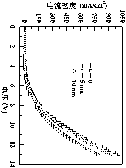
[0025] The electron transport passivation layer is one or more combinations of zirconium oxide, hafnium oxide, silicon oxide, alu...

Embodiment 2

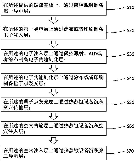
[0030] Embodiment two: if figure 2 As shown, a method for preparing a quantum dot light-emitting diode includes the following steps: S10, preparing a first conductive layer with a thickness of 5-200 nm on a glass substrate by magnetron sputtering; S20, passing Coating or printing to prepare an electron injection layer with a thickness of 10-300nm; S30, forming an electron transport passivation layer on the electron injection layer; S40, preparing a thickness of 5-200nm quantum dot light-emitting layer; S50, depositing a hole transport layer with a thickness of 5-200nm on the quantum dot light-emitting layer by thermal evaporation equipment; S60, depositing a hole transport layer on the hole transport layer by thermal evaporation The equipment deposits a hole injection layer with a thickness of 5-200 nm; S70, depositing a second conductive layer with a thickness of 5-200 nm on the hole injection layer by thermal evaporation equipment.

[0031] Wherein, in the step S30, the el...


PUM

PropertyMeasurementUnit
Thicknessaaaaaaaaaa
Thicknessaaaaaaaaaa
Thicknessaaaaaaaaaa

Abstract

The invention relates to the technical field of a light emitting diode, and specifically provides a quantum dot light emitting diode and a preparation method thereof. The quantum dot light emitting diode comprises a glass substrate, and a first conductive layer, an electron injection layer, a quantum dot light emitting layer, a hole transport layer, a hole injection layer and a second conductive layer which are stacked on the glass substrate in sequence; and an electron transfer passivation layer is also arranged between the quantum dot light emitting layer and the electron injection layer. Byadding the electron transfer passivation layer between the quantum dot light emitting layer and the electron injection layer, the problem of imbalance current carrier mobility efficiency between theelectron injection layer and the hole transport layer can be solved, the current efficiency of the light emitting device is improved effectively, and the current efficiency of the light emitting device achieves the optimal state.

Description

technical field [0001] The invention relates to the technical field of light emitting diodes, in particular to a quantum dot light emitting diode and a preparation method thereof. Background technique [0002] Quantum dot light-emitting diodes (QLEDs) have received extensive attention in the field of lighting and display devices due to their advantages such as high brightness, wide color gamut, low power consumption, easy processing, and flexibility. After more than 30 years of research, QLEDs The technology has made a huge leap, and its external quantum efficiency of red and green light has reached 20%. [0003] The development and progress of quantum dot light-emitting diodes is inseparable from the use of inorganic oxide electron injection layer or transport layer. At present, the most common electron injection or transport layer used in quantum dot light-emitting diodes is zinc oxide nanoparticles, which have high electron mobility. Rate. Due to the inherent characteri...

Claims


Application Information

Patent Timeline
IPC IPC(8): H01L51/50H01L51/56
CPCH10K50/115H10K50/14H10K50/18H10K71/00
Inventor 李山谢志强任思雨苏君海李建华
Owner TRULY HUIZHOU SMART DISPLAY
Why Eureka
Try Eureka