Forming method for fin-type field-effect tube

A technology of fin field effect transistors and fins, which is applied in the direction of electrical components, semiconductor/solid-state device manufacturing, circuits, etc., can solve the problems that the electrical performance of semiconductor devices needs to be improved, improve reliability and electrical performance, and avoid tip discharge Problems, improve the effect of the interface state

Inactive Publication Date: 2018-04-17
SEMICON MFG INT (SHANGHAI) CORP +1
View PDF5 Cites 5 Cited by
  • Summary
  • Abstract
  • Description
  • Claims
  • Application Information

AI Technical Summary

Problems solved by technology

[0004] However, the electrical performance of semiconductor devices formed by the prior art needs to be improved

Method used


Image

  • Forming method for fin-type field-effect tube
  • Forming method for fin-type field-effect tube
  • Forming method for fin-type field-effect tube

Examples


Embodiment Construction

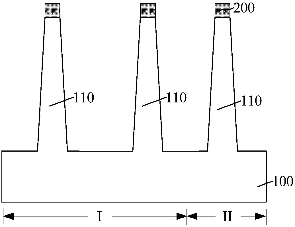
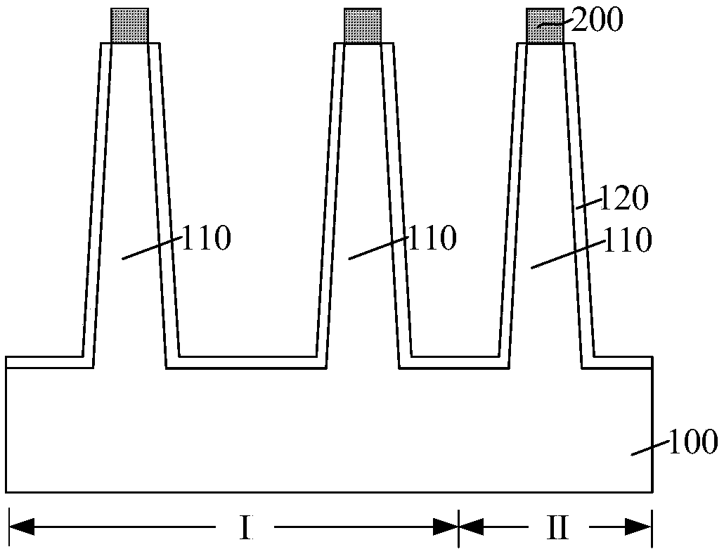
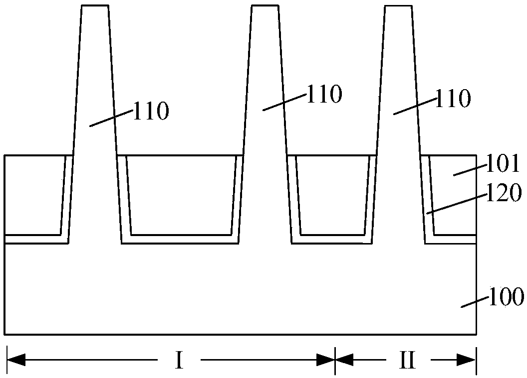
[0030] It can be seen from the background art that the electrical performance of the fin field effect transistor formed in the prior art needs to be improved. Analyze the reasons for this:

[0031] The gate dielectric layer of the FinFET includes a gate oxide layer covering the top surface and the sidewall surface of the fin, and the quality of the gate oxide layer has an important influence on the performance of the FinFET. Since there is a corner area (corner) on the top of the fin, the interface state between the gate oxide layer and the fin in the corner area is poor, and the sharp corner of the corner area is likely to cause the problem of tip discharge, thereby affecting the fin field effect. The electrical performance and reliability of the tube pose great challenges, such as gate oxide integrity (GOI, Gate Oxide Integrity), dielectric and time-dependent breakdown performance (TDDB, TimeDependent Dielectric Breakdown), positive temperature-instability characteristics ( ...


PUM


Abstract

The invention discloses a forming method for a fin-type field-effect tube, and the method comprises the steps: providing a substrate which is provided with a plurality of split fin parts, wherein thefin parts are provided with first atoms; forming a pseudo-gate structure which stretches across the fin parts and covers the top surfaces and side wall surfaces of a part of fin parts, and comprises agate oxidation layer and a pseudo-gate electrode layer located on the gate oxidation layer; removing a part of the pseudo-gate electrode layer by certain thickness; carrying out the annealing processing of the tops of the fin parts through the gas comprising second atoms after the part of the pseudo-gate electrode layer is removed, wherein the second atoms can form chemical bonds with the first atoms in the annealing processing. According to the invention, after the part of the pseudo-gate electrode layer is removed, the gas comprising second atoms is employed for the annealing processing ofthe tops of the fin parts. Because the second atoms can form chemical bonds with the first atoms in the annealing processing, the annealing processing is suitable for the reduction of the semiconductor atom dangling bonds in corner regions of the tops of the fin parts (such as a silicon atom dangling bond), improves the interface state between the gate oxidation layer and the fin parts, and solvesa problem of pea discharge caused by the sharp corners of the corner regions.

Description

technical field [0001] The invention relates to the field of semiconductors, in particular to a method for forming a fin field effect transistor. Background technique [0002] In semiconductor manufacturing, with the development trend of VLSI, the feature size of integrated circuits continues to decrease. In order to accommodate the reduction in feature size, the channel length of MOSFETs has also been shortened accordingly. However, as the channel length of the device is shortened, the distance between the source and the drain of the device is also shortened, so the control ability of the gate to the channel becomes worse, and the gate voltage pinches off the channel. The difficulty is also increasing, making the phenomenon of subthreshold leakage (subthreshold leakage), the so-called short-channel effect (SCE: short-channel effects) more likely to occur. [0003] Therefore, in order to better adapt to the reduction of the feature size, the semiconductor process gradually...

Claims


Application Information

Patent Timeline
Patent Type & Authority Applications(China)
IPC IPC(8): H01L21/336H01L29/78
CPCH01L29/66545H01L29/66795H01L29/785
Inventor 李勇
Owner SEMICON MFG INT (SHANGHAI) CORP
Why Eureka
Try Eureka