Method for improving radiation resistance capability of VDMOS device

An anti-irradiation and device technology, applied in semiconductor devices, semiconductor/solid-state device manufacturing, electrical components, etc., can solve problems such as difficulty in meeting process requirements, reduce density, reduce defect density, and inhibit the generation of interface states. Effect

Inactive Publication Date: 2017-05-31
NO 47 INST OF CHINA ELECTRONICS TECH GRP
View PDF2 Cites 1 Cited by
  • Summary
  • Abstract
  • Description
  • Claims
  • Application Information

AI Technical Summary

Problems solved by technology

However, the directly grown nitrided oxide gate has self-limiting growth characteristics, which is difficult to meet the requirements of the process

Method used


Image

  • Method for improving radiation resistance capability of VDMOS device

Examples


Embodiment 1

[0030] The preparation process of the three-layer structure grid in this embodiment is as follows:

[0031] (1) Use HF solution (water: HF=50:1) to clean the surface of the silicon wafer for 120 seconds to remove the oxide layer on the surface of the silicon wafer;

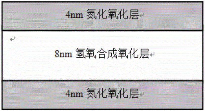
[0032] (2) After the silicon wafer is cleaned, rinsed and dried, a 4nm N 2 O Nitrided Gate Oxide. Compared with the conventional oxide gate dielectric, the nitrided gate dielectric can effectively improve the breakdown characteristics, suppress the hot carrier effect and improve the resistance to FN stress damage. At the same time, since nitriding promotes Si-N bonds to replace Si-O bonds, the formation of interface states is suppressed, which may improve the radiation resistance;

[0033] (3) The N prepared in step (2) at 800°C by hydrogen-oxygen synthesis oxidation method 2 An 8nm hydrogen-oxygen synthesis gate oxide layer was prepared on the O nitride gate oxide layer. due to H 2 -O 2 The temperature of syn...


PUM


Abstract

The invention discloses a method for improving radiation resistance capability of a VDMOS device, belongs to the technical field of manufacturing of a semiconductor. According to the method, a gate oxide layer in the VDMOS device is replaced by a three-layer-structured gate, so that the radiation resistance capability of the VDMOS device is improved; and the three-layer-structured gate consists of a nitrogen oxide layer, an oxyhydrogen synthesized oxide layer and a nitrogen oxide layer which are laminated in a recombination manner in sequence. The three-layer-structured gate oxide layer is manufactured by combination of two technologies of H<2>-O<2> synthesis and nitrogen gate oxide and by making the best of the two parties. Compared with conventional oxidization and H<2>-O<2> synthesis and oxidization, the radiation resistance capability of the VDMOS device can be improved by adoption of the method.

Description

technical field [0001] The invention relates to the technical field of semiconductor manufacturing, in particular to a method for improving the anti-radiation capability of a VDMOS device. Background technique [0002] During the flight in orbit, the spacecraft interacts with various charged particles (electrons and protons) in space. These electrons and protons have a strong impact on the performance of electronic devices used in spacecraft, causing ionizing radiation effects, displacement radiation effects, and single event effects. These radiation effects will lead to abnormalities or failures of electronic devices, and even eventually lead to catastrophic accidents in spacecraft. The research results at home and abroad show that different forms of failures will occur on the spacecraft in orbit, which shortens the working life and causes great losses. The results of fault analysis show that the radiation damage effect of space charged particles on electronic devices on ...

Claims


Application Information

Patent Timeline
Patent Type & Authority Applications(China)
IPC IPC(8): H01L21/285H01L21/3105H01L29/423H01L29/51B82Y30/00
CPCH01L29/401B82Y30/00H01L21/3105H01L29/42364H01L29/512H01L29/518
Inventor 任通郑莹
Owner NO 47 INST OF CHINA ELECTRONICS TECH GRP
Why Eureka
Try Eureka