CMOS transistor and manufacturing method thereof

A manufacturing method and transistor technology, applied in the direction of semiconductor devices, electrical components, circuits, etc., can solve the problems of increasing flicker noise, enhancing scattering, flicker noise interference, etc., and achieve the effect of reducing interface states and reducing dangling bonds

Inactive Publication Date: 2019-03-29
SHANGHAI HUALI INTEGRATED CIRCUTE MFG CO LTD
View PDF6 Cites 0 Cited by
  • Summary
  • Abstract
  • Description
  • Claims
  • Application Information

AI Technical Summary

Problems solved by technology

However, the introduction of nitrogen enhances the scattering of carriers in the channel, which intensifies the jitter of the channel current at low frequencies, thus increasing the flicker noise at low frequencies.
[0008] The increase of flicker noise causes lateral interference to the device at low frequencies, thus affecting the sensitivity at low frequencies
At present, logic devices in the industry, especially mobile phone chips, are gradually developing towards the system-on-chip (SOC). The CPU, IO controller, Ram controller, audio circuit and even the baseband chip are all integrated on one SOC. The existence of flicker noise will affect the The filtering ability of the baseband under clutter will cause the call to be unsmooth under the weak signal of the mobile phone and affect the effect
At the same time, the integrated audio circuit will seriously affect its signal-to-noise ratio (db) and affect the experience of mobile phones. Therefore, the industry's control over flicker noise is getting higher and higher.

Method used


Image

  • CMOS transistor and manufacturing method thereof

Examples


Embodiment Construction

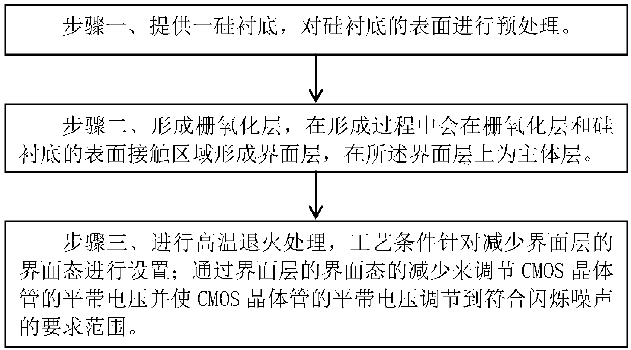
[0042] The device of the embodiment of the present invention is obtained on the basis of an in-depth analysis of the technical problems existing in the existing CMOS transistor, so before introducing the device of the embodiment of the present invention in detail, first introduce the technical problems of the existing CMOS transistor:

[0043]In the 28HP process, HKMG is usually used, but in the 28LP process, the complex HKMG is not used, and the structure of gate oxide layer plus polysilicon gate is still used. The gate oxide layer is mainly composed of SiO2, and usually includes nitrogen element, namely SiON. In the gate oxide layer of CMOS transistors, SiO 2 The interface with the silicon substrate, that is, Si, is the boundary of silicon single crystal, that is, there is an interface layer of Si-SiO2. Studies have shown that Si-SiO 2 The interface layer is not a geometric plane, but there is about thickness of. The structure of the interface layer is SiO x , where x is...


PUM

PropertyMeasurementUnit
thicknessaaaaaaaaaa

Abstract

The invention discloses a CMOS transistor, which comprises a gate oxide layer formed on the surface of a silicon substrate. The gate oxide layer comprises an interface layer formed on the surface of the silicon substrate and a main layer located on the interface layer. The interface layer has a SiOx structure, wherein x is between 1 and 2. The main layer includes a SiO2 layer. Before the formationof the interface layer, the surface of the silicon substrate has a pretreated structure for reducing the interface state of the interface layer. After the formation of the gate oxide layer, the interface layer is annealed at high temperature to reduce the interface state of the interface layer. The flat-band voltage of the CMOS transistor is adjusted by reducing the interface state of the interface layer, and the flat-band voltage of the CMOS transistor is adjusted to a range required for scintillation noise. The invention further discloses a manufacturing method of the CMOS transistor. The interface state of the gate oxide layer can be reduced and controlled, and therefore, the scintillation noise of the device can be reduced.

Description

technical field [0001] The invention relates to the field of manufacturing semiconductor integrated circuits, in particular to a CMOS transistor; the invention also relates to a method for manufacturing the CMOS transistor. Background technique [0002] As the requirements for device performance become higher and higher, the size of the device process becomes smaller and smaller. For example, the process node in the existing semiconductor integrated circuit manufacturing is below 28nm. Correspondingly, as the process size becomes smaller and smaller, the device becomes smaller and smaller, which leads to the thinner and thinner of the most critical gate oxide layer (gate oxide), and when the gate oxide layer is made from 3nm down, Basically, for every 0.5nm drop, the leakage current of the device will increase by two orders of magnitude. [0003] The 28nm process node includes the 28LP process, that is, the 28nm low power (LP) process, which requires the thickness of the el...

Claims


Application Information

Patent Timeline
Patent Type & Authority Applications(China)
IPC IPC(8): H01L29/423H01L29/51H01L21/28
CPCH01L29/401H01L29/42364H01L29/518
Inventor 成鑫华康俊龙
Owner SHANGHAI HUALI INTEGRATED CIRCUTE MFG CO LTD
Why Eureka
Try Eureka