Semiconductor device and forming method thereof

A technology for semiconductors and devices, applied in the field of semiconductor devices and their formation, can solve the problem that the electrical properties of semiconductor structures need to be improved, and achieve the effects of improving electrical properties, strong protection, and good hole filling properties.

Active Publication Date: 2018-04-24
SEMICON MFG INT (SHANGHAI) CORP +1
View PDF3 Cites 10 Cited by
  • Summary
  • Abstract
  • Description
  • Claims
  • Application Information

AI Technical Summary

Problems solved by technology

[0004] Although the introduction of high-k metal gates can improve the electrical properties of semiconductor structures to a certain extent, the electrical properties of semiconductor structures formed by existing technologies still need to be improved.

Method used


Image

  • Semiconductor device and forming method thereof
  • Semiconductor device and forming method thereof
  • Semiconductor device and forming method thereof

Examples


Embodiment Construction

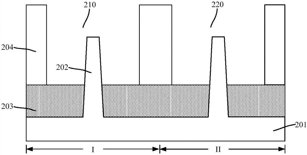
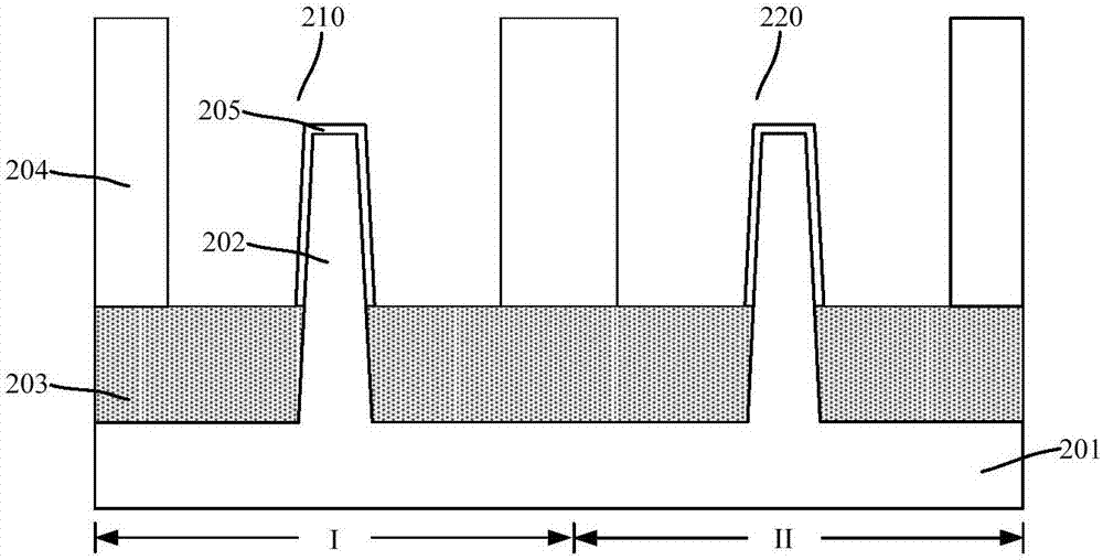
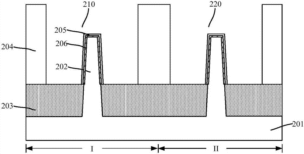
[0030] According to the background art, the electrical performance of semiconductor devices formed in the prior art needs to be improved.

[0031] After research, it is found that in order to meet the requirements of NMOS transistors and PMOS transistors to improve the threshold voltage (Threshold Voltage), different metal materials are usually used as the work function (WF, WorkFunction) layer materials in the gate structures of NMOS transistors and PMOS transistors. The material of the N-type work function layer in the tube may be called an N-type work function material, and the material of the P-type work function layer in the PMOS tube may be called a P-type work function material. For NMOS tubes, there are ions in the metal grid that are easy to diffuse into the N-type work function layer. For example, the metal grid contains F ions, and the F ions diffuse into the N-type work function layer will cause N-type work function. The equivalent work function value of the functi...


PUM

PropertyMeasurementUnit
thicknessaaaaaaaaaa
thicknessaaaaaaaaaa
thicknessaaaaaaaaaa

Abstract

A semiconductor device and a forming method thereof are provided. The forming method includes the following steps: providing a substrate including an NMOS region, wherein an interlayer dielectric layer is formed on the substrate, and an N region opening penetrating the interlayer dielectric layer is formed in the interlayer dielectric layer of the NMOS region; forming a high-k gate dielectric layer on the bottom and sidewall of the N region opening; forming an N-type work function layer on the high-k gate dielectric layer; forming a diffusion barrier layer on the N-type work function layer; hydrogenating the diffusion barrier layer; and after hydrogenation, forming a metal gate filling the N region opening on the diffusion barrier layer. The ability of the diffusion barrier layer to protect the N-type work function layer is improved, and therefore, the electrical performance of a semiconductor device formed is improved.

Description

technical field [0001] The invention relates to the technical field of semiconductor manufacturing, in particular to a semiconductor device and a forming method thereof. Background technique [0002] The main semiconductor device of an integrated circuit, especially a very large scale integrated circuit, is a metal-oxide-semiconductor field effect transistor (MOS transistor). With the continuous development of integrated circuit manufacturing technology, the technology nodes of semiconductor devices are continuously reduced, and the geometric dimensions of semiconductor structures are continuously reduced following Moore's law. When the size of the semiconductor structure is reduced to a certain extent, various secondary effects caused by the physical limit of the semiconductor structure appear one after another, and it becomes more and more difficult to scale down the feature size of the semiconductor structure. Among them, in the field of semiconductor manufacturing, the ...

Claims


Application Information

Patent Timeline
Patent Type & Authority Applications(China)
IPC IPC(8): H01L21/8238H01L27/092
CPCH01L21/823878H01L27/092H01L21/823842H01L21/28088H01L21/3003H01L29/66545H01L21/02304H01L21/2253H01L21/28026H01L21/823814H01L29/42372
Inventor 李勇
Owner SEMICON MFG INT (SHANGHAI) CORP
Why Eureka
Try Eureka