Eureka AIR delivers breakthrough ideas for toughest innovation challenges, trusted by R&D personnel around the world.

Static protection structure in monolithic microwave integrated circuit and manufacturing method of static protection structure

A microwave integrated circuit and electrostatic protection technology, which is applied in the direction of circuit, semiconductor/solid-state device manufacturing, electrical components, etc., can solve the problems of limited integrated circuit layout area, large integrated circuit area, waste, etc., and achieve the effect of saving layout area

Active Publication Date: 2018-05-04
XIAMEN SANAN INTEGRATED CIRCUIT
View PDF6 Cites 1 Cited by
  • Summary
  • Abstract
  • Description
  • Claims
  • Application Information

AI Technical Summary

Problems solved by technology

The disadvantage of the above structure is that the area of ​​the integrated circuit to be occupied by the diode string is relatively large
For the current nm-level process technology, the layout area of ​​the integrated circuit is very limited. If a large amount of area is occupied by the diode string, it will undoubtedly cause a lot of waste.

Method used


Image

  • Static protection structure in monolithic microwave integrated circuit and manufacturing method of static protection structure
  • Static protection structure in monolithic microwave integrated circuit and manufacturing method of static protection structure
  • Static protection structure in monolithic microwave integrated circuit and manufacturing method of static protection structure

Examples


Embodiment 1

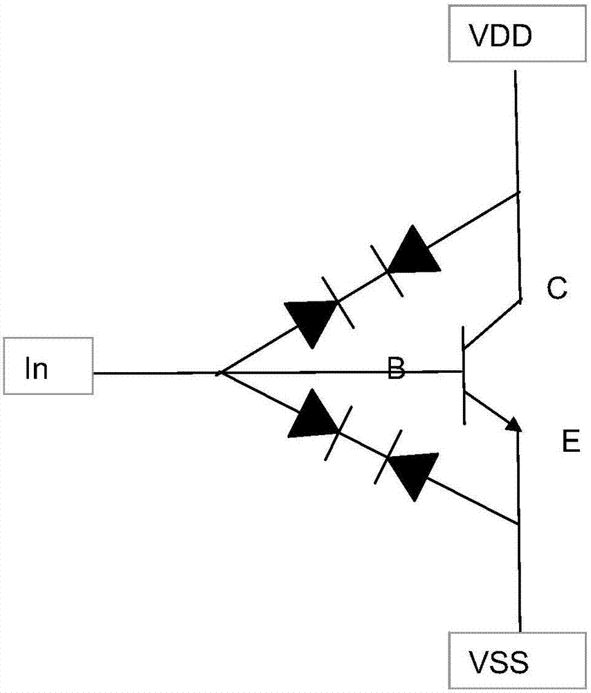
[0032] refer to figure 1 , the present embodiment provides an electrostatic protection structure in a monolithic microwave integrated circuit, in which diode groups arranged in a back-to-back structure are respectively arranged in parallel between the base region-the emitter region and the base region-the collector region of the HBT tube; each The diode group includes two diodes, and the anodes of the two diodes are connected to each other to form a back-to-back structure

[0033] When the chip is electrostatically discharged, the base area of ​​the HBT tube and the substrate form a large voltage difference, which will break down the base area of ​​the HBT tube. Therefore, add two reverse diodes connected in series near the base region and emitter region, base region and collector region. When electrostatic discharge occurs, no matter how the current flows, one of the two diodes will always conduct, so that The voltage difference between the base region and the substrate is c...

Embodiment 2

[0035] The difference between this embodiment and Embodiment 1 is that: the diode group includes two diodes, and the cathodes of the two diodes are connected to each other to form a back-to-back structure. The rest is the same as that of Embodiment 1, and the working principle is also consistent with that of Embodiment 1, so it will not be repeated here.

Embodiment 3

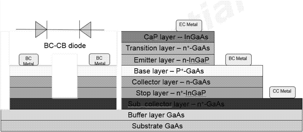
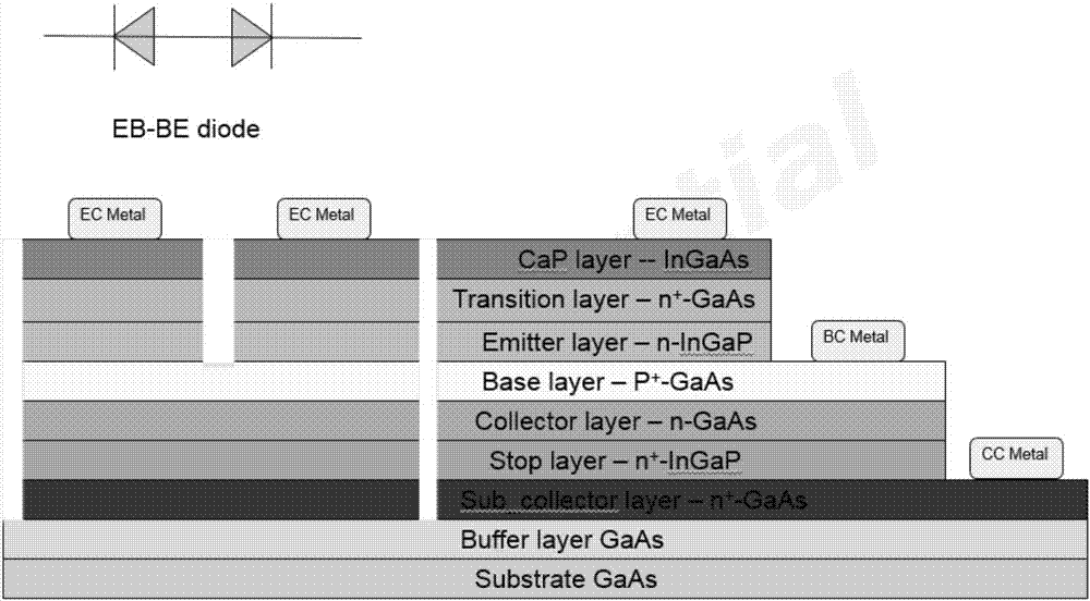
[0037] refer to figure 2 , the present embodiment provides a microstructure for electrostatic protection in a monolithic microwave integrated circuit, including at least one HBT tube prepared on a GaAs-based epitaxial wafer, and two diodes independent of the HBT tube are prepared on the GaAs-based epitaxial wafer ; Two diodes share a barrier n + -InGaP, and the two diodes are sequentially stacked on the barrier layer n + - Collector layer n-GaAs on InGaP, base layer p + -GaAs and emitter layer n + -GaAs; the collector layer n-GaAs of the two diodes to each other, the base layer p + -GaAs and emitter layer n + -GaAs are arranged independently of each other to form a back-to-back diode group with interconnected cathodes;

[0038] The anode BC Metal of one of the diodes is connected to the base area BC Metal of the HBT tube, and the anode BC Metal of the other diode is connected to the collector area CC Metal of the HBT tube; or, the anode BC Metal of one of the diodes is con...


PUM


Abstract

The invention provides a static protection structure in a monolithic microwave integrated circuit. Diode groups are respectively arranged in parallel between a base region and an emitter region and between the base region and a current collector region of a transistor and are arranged in a back-to-back structure, each diode group comprises two diodes, and positive electrodes of the two diodes areconnected or negative electrodes of the two diodes are connected to form the back-to-back structure. The invention provides the static protection structure in the monolithic microwave integrated circuit, and the occupancy area of the static protection structure in the integrated circuit is effectively reduced. The invention also provides a manufacturing method of the static protection structure.

Description

technical field [0001] The invention relates to the field of integrated circuits, in particular to an electrostatic protection structure in integrated circuits. Background technique [0002] The phenomenon of electrostatic discharge (ESD) in nature poses a serious threat to the reliability of integrated circuits. In the industry, 30% of the failures of integrated circuit products are caused by electrostatic discharge, and the increasingly smaller process size, thinner gate oxide thickness, and base area all make integrated circuits more likely to be damaged by electrostatic discharge greatly increase. Therefore, improving the reliability of integrated circuit electrostatic discharge protection has a non-negligible effect on improving the yield of products. [0003] The modes of electrostatic discharge phenomena are usually divided into four types: HBM (Human Body Model), MM (Machine Discharge Model), CDM (Component Charge Discharge Model) and Field Induction Model (FIM). ...

Claims


Application Information

Patent Timeline
IPC IPC(8): H01L27/02H01L21/82
CPCH01L21/82H01L27/0255H01L27/0266
Inventor 魏鸿基许燕丽王江朱庆芳
Owner XIAMEN SANAN INTEGRATED CIRCUIT
Why Eureka
Eureka Blog
Learn More