Preparation method of field effect transistor based on two-dimensional gallium selenide material

A field effect transistor, target material technology, applied in semiconductor devices, final product manufacturing, sustainable manufacturing/processing, etc., can solve problems such as low production efficiency, achieve the effect of simple method, avoid glue residue, and reduce process steps

Active Publication Date: 2018-05-04
NORTHWESTERN POLYTECHNICAL UNIV
View PDF5 Cites 8 Cited by
  • Summary
  • Abstract
  • Description
  • Claims
  • Application Information

AI Technical Summary

Problems solved by technology

[0007] In order to overcome the deficiency of low preparation efficiency of the existing field-effect transistor preparation method

Method used


Image

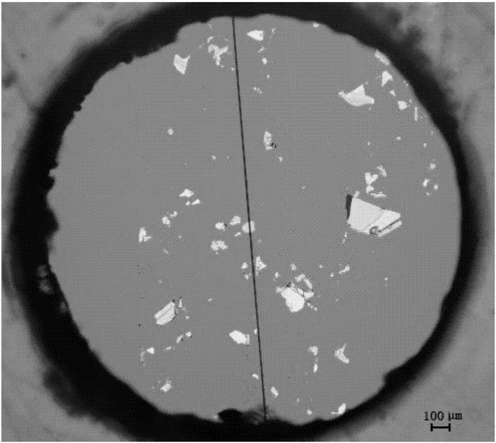
  • Preparation method of field effect transistor based on two-dimensional gallium selenide material
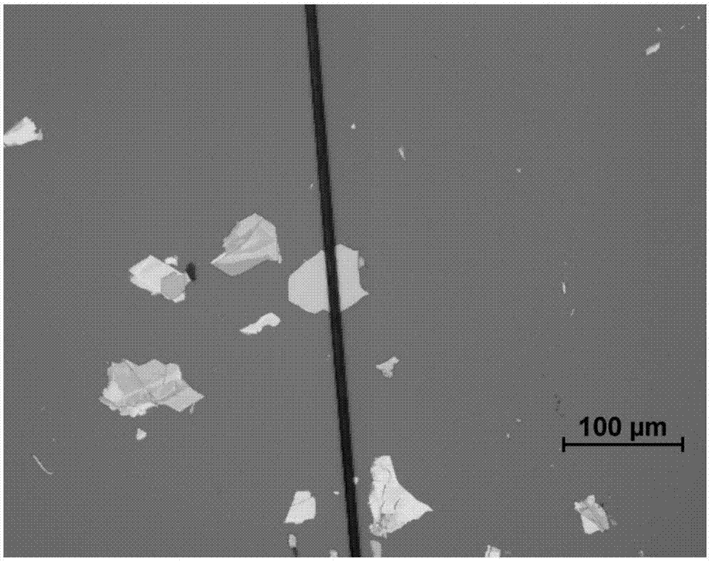
  • Preparation method of field effect transistor based on two-dimensional gallium selenide material
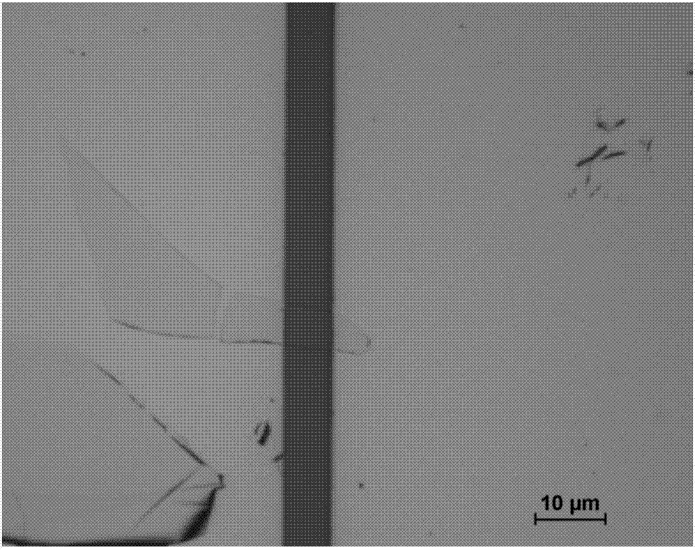
  • Preparation method of field effect transistor based on two-dimensional gallium selenide material

Examples


Embodiment 1

[0027] Step 1. A high-quality GaSe single crystal is grown by the vertical Bridgman method, a GaSe bulk material with a smooth surface and no defects is selected, and a GaSe thin layer with a thickness of 15 μm is obtained by cleavage along its cleavage plane.

[0028] Step 2: Attach the GaSe thin layer to the Scotch tape evenly, fold the tape in half and tear it off quickly, and repeat the operation 6 times until the material on the tape is dull and colorless.

[0029] Step 3: Adhere the tape with the GaSe material evenly to PDMS (polydimethylsiloxane) with a thickness of 0.5 mm, and peel off the PDMS to obtain two-dimensional GaSe materials with different thicknesses. To obtain thinner GaSe materials, the tape should be peeled off quickly in one direction.

[0030] Step 4: Under an optical microscope, find a two-dimensional GaSe with a uniform thickness and a size of 30 μm×60 μm as a target material for transfer. Use a puncher to punch a round hole with a diameter of 3mm on...

Embodiment 2

[0040] Step 1. A high-quality GaSe single crystal is grown by the vertical Bridgman method, a GaSe bulk material with a smooth surface and no defects is selected, and a GaSe thin layer with a thickness of 10 μm is obtained by cleavage along its cleavage plane.

[0041] Step 2: Attach the GaSe thin layer to the Scotch tape evenly, fold the tape in half and tear it off quickly, repeat the operation 8 times until the material on the tape is dull and colorless.

[0042] Step 3: Adhere the tape with the GaSe material evenly to PDMS (polydimethylsiloxane) with a thickness of 0.5 mm, and peel off the PDMS to obtain two-dimensional GaSe materials with different thicknesses. To obtain thinner GaSe materials, the tape should be peeled off quickly in one direction.

[0043] Step 4: Under an optical microscope, find a two-dimensional GaSe with a uniform thickness and a size of 6 μm×21 μm as a target material for transfer. Punch a circular hole with a diameter of 2mm on the tape with a pu...

Embodiment 3

[0052] Step 1. A high-quality GaSe single crystal is grown by the vertical Bridgman method, a GaSe bulk material with a smooth surface and no defects is selected, and a GaSe thin layer with a thickness of 13 μm is obtained by cleavage along its cleavage plane.

[0053] Step 2: Attach the GaSe thin layer to the Scotch tape evenly, fold the tape in half and tear it off quickly, repeat the operation 7 times until the material on the tape is dull and colorless.

[0054] Step 3: Adhere the tape with the GaSe material evenly to PDMS (polydimethylsiloxane) with a thickness of 0.5 mm, and peel off the PDMS to obtain two-dimensional GaSe materials with different thicknesses. To obtain thinner GaSe materials, the tape should be peeled off quickly in one direction.

[0055] Step 4: Under an optical microscope, find a two-dimensional GaSe with a uniform thickness and a size of 12 μm×18 μm as a target material for transfer. Punch a round hole with a diameter of 2.5mm on the tape with a pu...


PUM

PropertyMeasurementUnit
Thicknessaaaaaaaaaa

Abstract

The invention discloses a preparation method of a field effect transistor based on a two-dimensional gallium selenide material, and is used for solving the technical problem that an existing field effect transistor preparation method is low in preparation efficiency. According to the technical scheme, under a microscope and a three-dimensional aligning-transferring platform, the material is transferred onto a silicon substrate with the aid of PDMS, influence of adhesive residues to devices can be avoided effectively, a mask can be prepared from carbon fibers and PDMS, and then is provided witha metal electrode in an evaporation manner, a straight channel with the size about 4-7 mu m can be prepared, and a material with the smaller size (greater than or equal to 10 mu m) can be prepared into the field effect transistor. The preparation method of the two-dimensional GaSe field effect transistor is simple to operate and low in cost, and is convenient and speedy; the material is not injured; and the preparation efficiency of the field effect transistor is improved.

Description

technical field [0001] The invention relates to a method for preparing a field effect transistor, in particular to a method for preparing a field effect transistor based on a two-dimensional gallium selenide material. Background technique [0002] Since the discovery of graphene in 2004, two-dimensional materials have attracted widespread attention due to their unique physical and chemical properties and their great research value. Field-effect transistors based on two-dimensional GaSe materials also show great application prospects in the field of photodetectors due to their high photoresponsivity, high external quantum efficiency and other excellent properties. At present, the commonly used method for preparing field effect transistors based on two-dimensional materials is to prepare a mask by photolithography or copper mesh, and then combine with evaporation technology to prepare electrodes. [0003] Document 1 "Huang H, Wang P, Gao Y, et al. Highly sensitive phototransi...

Claims


Application Information

Patent Timeline
IPC IPC(8): H01L31/18H01L31/112H01L31/032
CPCH01L31/032H01L31/112H01L31/18Y02P70/50
Inventor 王涛李洁赵清华张颖菡殷子昂王维介万奇
Owner NORTHWESTERN POLYTECHNICAL UNIV
Why Eureka
Try Eureka