Light guide plate packaging structure for microstructure array with surface having quantum dots and manufacturing method thereof
A technology of microstructure array and packaging structure, which is applied in the directions of plane/plate light guides, light guides of lighting systems, light guides, etc., can solve the problems of reducing the luminous performance of quantum dots, and solve the problems of preparation and integrated packaging, and the process flow is complete. , The effect of good water and oxygen barrier ability
- Summary
- Abstract
- Description
- Claims
- Application Information
AI Technical Summary
Problems solved by technology
Method used
Image

Examples
Embodiment 1
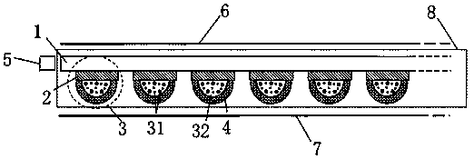
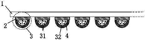
[0032] image 3 The encapsulation structure of the light guide plate with the quantum dot microstructure array on the surface is shown, which includes a light guide plate substrate layer 1 , a barrier layer 2 , a quantum dot microstructure array dimming layer 3 , and an encapsulation layer 4 . exist image 3 In the first initial structure shown in , the quantum dot microstructure array dimming layer 3 is composed of quantum dots 31 and composite materials 32 . The quantum dot microstructure array contains one or more quantum dots and composite scattering materials with a central wavelength between 380-780nm. It is made by mixing quantum dots and composite scattering materials in a certain proportion to form a quantum dot slurry. Its ratio can be determined according to needs. The quantum dot microstructure array is formed by inkjet printing method. The thickness of the quantum dot microstructure array is 20-50 μm. The shape of the quantum dot microstructure array can be hemis...
Embodiment 2
[0037] Figure 5 The encapsulation structure of the light guide plate with the quantum dot microstructure array on the surface is shown, which includes a light guide plate substrate layer 1 , a barrier layer 2 , a quantum dot microstructure array dimming layer 3 , and an encapsulation layer 4 . The quantum dot microstructure array dimming layer 3 is composed of quantum dots 31 and composite materials 32. The preparation and formation of the quantum dot microstructure array is similar to that in Embodiment 1 of the present invention, and will not be repeated here. Outside the dimming layer of the quantum dot microstructure array is the encapsulation layer, which can be coated by spin coating or pulling method, but not limited to these methods. The material of the encapsulation layer is specifically made of inorganic materials such as silicon dioxide, silicon oxynitride, oxide Composed of aluminum, its thickness is 15-25 μm. Figure 5 Middle 5 is a mask plate, which is placed u...
Embodiment 3
[0043] Figure 7 The encapsulation structure of the light guide plate with the quantum dot microstructure array on the surface is shown, which includes a light guide plate substrate layer 1 , a barrier layer 2 , a quantum dot microstructure array dimming layer 3 , and an encapsulation layer 4 . exist image 3 The initial structure shown in the figure modifies the formation position of the quantum dot network. The quantum dot microstructure array can be embedded in the concave groove on the lower surface of the light guide plate. The groove can be formed by laser etching or hot pressing, and the quantum dot The dot paste is printed in the groove by screen printing, transfer printing or inkjet printing, and after the quantum dot microstructure array is cured, a packaging layer is printed by point-to-point screen printing or inkjet printing overprinting, or After the quantum dots are solidified, directly spin coat or pull a layer of encapsulation layer, Figure 8 is a schematic...
PUM
| Property | Measurement | Unit |
|---|---|---|
| Viscosity | aaaaa | aaaaa |
| Surface tension | aaaaa | aaaaa |
| Thickness | aaaaa | aaaaa |
Abstract
Description
Claims
Application Information
 - R&D
- Intellectual Property
- Life Sciences
- Materials
- Tech Scout
- Unparalleled Data Quality
- Higher Quality Content
- 60% Fewer Hallucinations
Browse by: Latest US Patents, China's latest patents, Technical Efficacy Thesaurus, Application Domain, Technology Topic, Popular Technical Reports.
© 2025 PatSnap. All rights reserved.Legal|Privacy policy|Modern Slavery Act Transparency Statement|Sitemap|About US| Contact US: help@patsnap.com