An optimum imaging plane adjusting and calibrating method based on a CCD coherence factor detection apparatus

A detection device and coherence factor technology, which is applied in the photoplate-making process exposure device, the photo-plate-making process of the pattern surface, optics, etc., can solve the problems that the calibration process is difficult to achieve, and the production process cannot meet the requirements of real-time measurement of the lighting system. Achieve the effects of shortening the photosensitive time, high reusability, and improving detection efficiency

Inactive Publication Date: 2018-05-15
SICHUAN UNIV
View PDF5 Cites 0 Cited by
  • Summary
  • Abstract
  • Description
  • Claims
  • Application Information

AI Technical Summary

Problems solved by technology

The disadvantage of these methods is that after the whole system is integrated, it is measured at the silicon wafer
Aberration-corrected optical system, only when the wave aberration does not exceed (Depend on arrive ), the image quality can be accepted, the traditional calibration process is difficult to achieve this accuracy, and because of the need to expose the photoresist, it greatly increases the production cost, so this series of conditions all show that the traditional production The process cannot meet the requirements of real-time measurement during the development of the lighting system

Method used


Image

  • An optimum imaging plane adjusting and calibrating method based on a CCD coherence factor detection apparatus
  • An optimum imaging plane adjusting and calibrating method based on a CCD coherence factor detection apparatus
  • An optimum imaging plane adjusting and calibrating method based on a CCD coherence factor detection apparatus

Examples


Embodiment Construction

[0035] In order to make the purpose, technical solution and advantages of the present invention clearer, the present invention will be further described in detail below in conjunction with the accompanying drawings and embodiments. It is necessary to point out here that the embodiments described below are exemplary, and are intended to further explain the present invention, but can not be interpreted as limiting the protection scope of the present invention. Making some non-essential improvements and adjustments still belongs to the protection scope of the present invention.

[0036] The specific steps of an optimal imaging plane adjustment method based on a CCD coherence factor detection device proposed by the present invention are as follows:

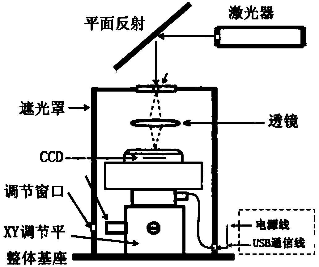
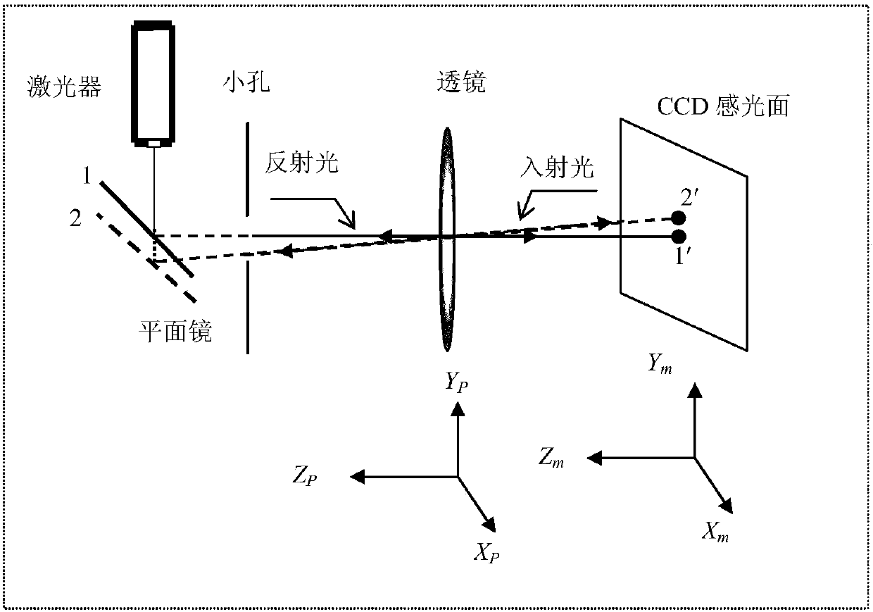
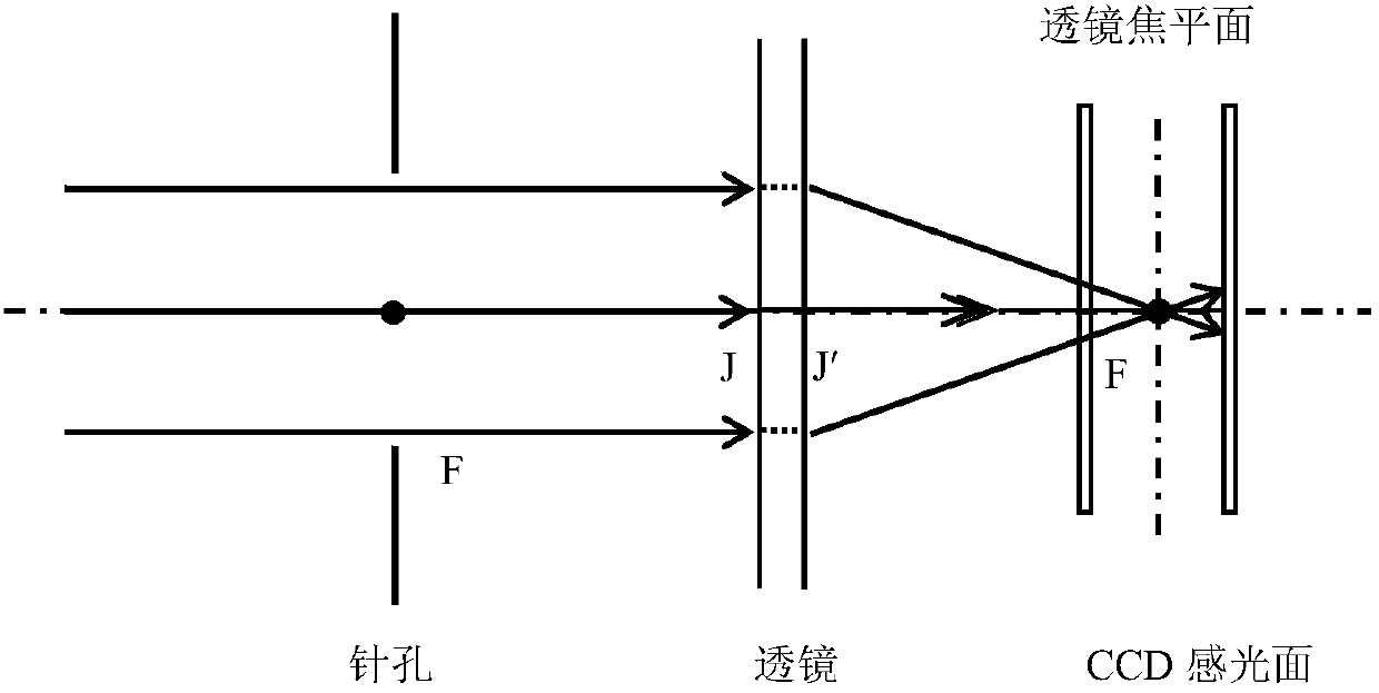
[0037] 1. Build the device for the detection system, such as figure 1 shown. The device consists of a laser, a mirror, a pinhole, a lens group, a manual X-Y displacement platform and a CCD. After calibration, the laser beam is inci...


PUM


Abstract

An optimum imaging plane adjusting and calibrating method based on a CCD coherence factor detection apparatus is provided. The apparatus is used for detecting an out-of-focus situation of a CCD in a lens in the axial direction in an optical projection exposure photoetching system, and includes a laser, a planar mirror, the lens, a CCD image sensor and a manually operated X-Y displacement platform.According to the method, firstly, the CCD is utilized to collect a laser spot image, the X-Y displacement platform is moved according to changes of a light spot and barycentric energy to achieve coarse adjustment, then a fine-adjustment evaluation function and a precise adjustment evaluation function are established respectively to move the X-Y displacement platform to achieve fine adjustment andprecise adjustment, and finally, calibration of the optimum imaging plane for the CCD is achieved. The method is simple to operate and high in detection sensitivity and increased in detection efficiency and reliability.

Description

technical field [0001] The invention relates to a detection device for the out-of-focus condition of a CCD in the lens axis of optical projection exposure lithography, especially capable of realizing the calibration of the best image plane of the CCD in the lens axis in the device. Background technique [0002] In the manufacture of integrated circuits, the process technology of using the principle of photochemical reaction to transfer the circuit pattern to the surface of the single crystal or the dielectric layer to form an effective pattern window or functional pattern is called photolithography. The scale of integrated circuits has developed rapidly from only a few dozen transistors per chip in the 1960s to 1 billion transistors today, and the support of lithography technology has played a critical role. Typical photolithography techniques include optical exposure lithography, X-ray lithography, electron beam lithography, and the like. At present, most of the semiconduc...

Claims


Application Information

Patent Timeline
Patent Type & Authority Applications(China)
IPC IPC(8): G03F7/20G03F9/00
CPCG03F7/70258G03F9/7026
Inventor 曹益平
Owner SICHUAN UNIV
Why Eureka
Try Eureka