Processing method for processing rectangular photovoltaic cell silicon slices through columnar crystal silicon rods
A photovoltaic cell silicon wafer and columnar crystal technology, applied in photovoltaic power generation, stone processing equipment, sustainable manufacturing/processing, etc., to achieve high photoelectric conversion efficiency, improve effective utilization, and reduce the cost of silicon wafers
- Summary
- Abstract
- Description
- Claims
- Application Information
AI Technical Summary
Problems solved by technology
Method used
Image

Examples
Embodiment 1
[0043] A processing method for processing rectangular photovoltaic cell silicon wafers with columnar crystal silicon rods, comprising the following steps:
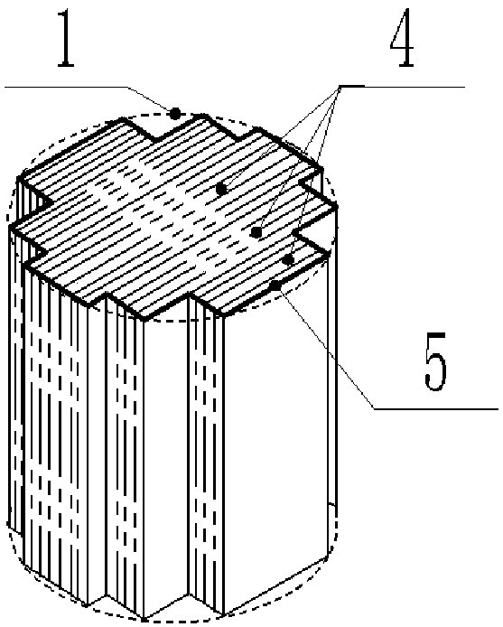
[0044] Step 1. Confirm and process the cylindrical surface of the silicon rod: process the cylindrical surface of the columnar crystal silicon rod to obtain the cylindrical surface of the crystal silicon rod. The directrix of the cylindrical surface of the crystal silicon rod is a closed curve or consists of several discontinuous curves Connected; Among them, the material of the columnar crystal silicon rod is polysilicon, and there is no requirement for the crystal direction;
[0045] Step 2, cut off the silicon rod: cut off the crystalline silicon rod according to the required length of the rectangular silicon chip, to determine the outline size of the rectangular silicon chip, and determine the standardized length of a group of opposite sides of the cut rectangular silicon chip;
[0046] Step 3, slicing: cutting the cry...
Embodiment 2
[0054] A processing method for processing rectangular photovoltaic cell silicon wafers with columnar crystal silicon rods, the schematic diagram of which is as follows figure 1 and figure 2 As shown, it includes the following steps:
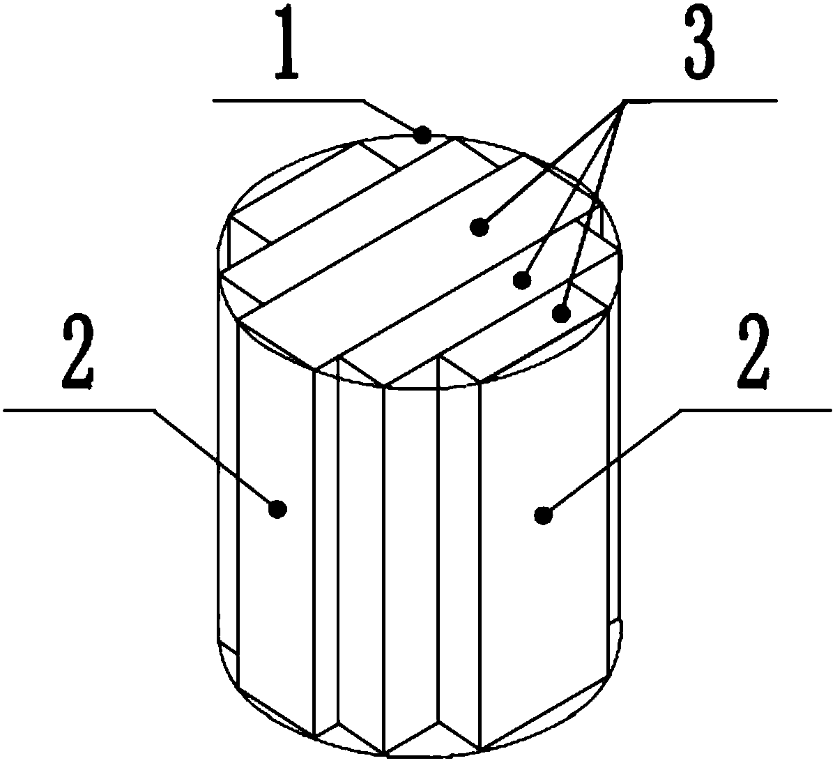
[0055] Step 1: According to the crystal direction of the required silicon wafer, cut off the edge skin on the cylindrical surface 1 of the crystal silicon rod to obtain the silicon block positioning plane 2;
[0056] Step 2: cut off the silicon rod according to the required length, and remove the unusable head and tail;
[0057] Step 3: Confirm the crystal orientation and vertical block to obtain a series of silicon blocks 3 with the same length and different widths;
[0058] Step 4: Remove the irregular sides and corners of the silicon block 3 to meet the requirements, and then chamfer the corners;
[0059] Step 5: Slicing the silicon blocks obtained in Step 4 into groups to obtain silicon wafers 4 .
[0060] In this embodiment, the equival...
Embodiment 3
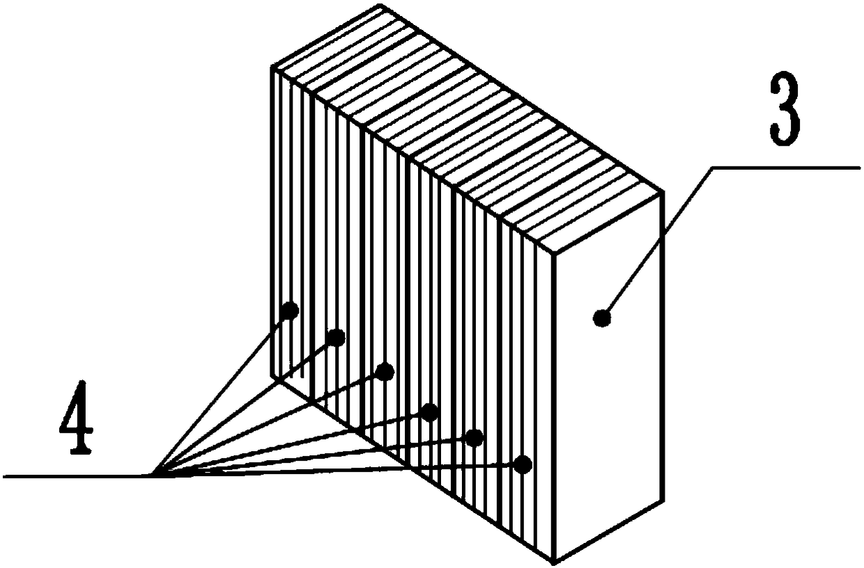
[0062] A processing method for processing rectangular photovoltaic cell silicon wafers with columnar crystal silicon rods, the schematic diagram of which is as follows image 3 As shown, it includes the following steps:
[0063] Step 1: remove unusable head and tail materials, and process the cylindrical profile 5 of the silicon rod;
[0064] Step 2: cut off the silicon rod according to the required length, and then chamfer;
[0065] Step 3: Slicing the silicon block obtained in Step 2 to obtain a silicon wafer 4 .
[0066] In this embodiment, the crystal orientations of the crystalline silicon rods and silicon slices are not controlled, and the crystalline silicon rods may be polycrystalline silicon. Example 4.
PUM
 Abstract
Description
Claims
Application Information
 - Generate Ideas
- Intellectual Property
- Life Sciences
- Materials
- Tech Scout
- Unparalleled Data Quality
- Higher Quality Content
- 60% Fewer Hallucinations
Browse by: Latest US Patents, China's latest patents, Technical Efficacy Thesaurus, Application Domain, Technology Topic, Popular Technical Reports.
© 2025 PatSnap. All rights reserved.Legal|Privacy policy|Modern Slavery Act Transparency Statement|Sitemap|About US| Contact US: help@patsnap.com