
Tmbs device and manufacturing method thereof

A manufacturing method and device technology, applied in semiconductor/solid-state device manufacturing, semiconductor devices, electrical components, etc., can solve problems such as large reverse leakage current, adverse effects of device reverse breakdown voltage, etc., and achieve reverse breakdown voltage Hold, eliminate the influence of reverse breakdown voltage, and maintain the effect of forward voltage

Active Publication Date: 2020-11-20
SHANGHAI HUAHONG GRACE SEMICON MFG CORP
View PDF4 Cites 0 Cited by
  • Summary
  • Abstract
  • Description
  • Claims
  • Application Information

AI Technical Summary

Problems solved by technology

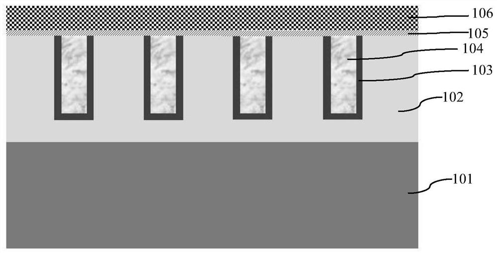
However, when silicon dioxide is used to form the gate dielectric layer 103, it is easy to generate a large reverse leakage current (Reverse I, IR)
However, when the gate dielectric layer 103 is changed to other single materials, it will adversely affect the reverse breakdown voltage of the device.

Method used


Image

  • Tmbs device and manufacturing method thereof
  • Tmbs device and manufacturing method thereof
  • Tmbs device and manufacturing method thereof

Examples


Embodiment Construction

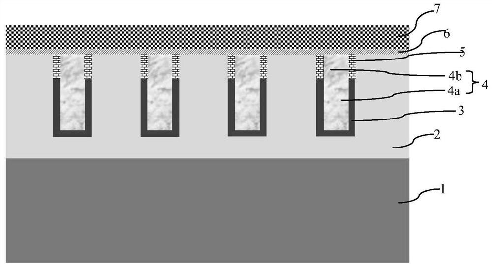
[0052] Such as figure 2 Shown, is the structural representation of the TMBS device of the embodiment of the present invention; The TMBS device of the embodiment of the present invention comprises:

[0053] A plurality of trench gate structures are formed in the N-type epitaxial layer 2, each of the trench gate structures includes a trench and a gate dielectric layer is formed on the inner surface of each of the trenches, and a gate dielectric layer is formed on the inner surface of the trench. The polysilicon gate 4 in each trench of the gate dielectric layer. Preferably, the N-type epitaxial layer 2 is formed on an N-type semiconductor substrate; the semiconductor substrate is a silicon substrate, and the N-type epitaxial layer 2 is a silicon epitaxial layer.

[0054] The gate dielectric layer is divided into two parts, the first part is a first gate dielectric layer 3 composed of a silicon dioxide layer, and the first gate dielectric layer 3 is formed on the bottom surface...


PUM


Abstract

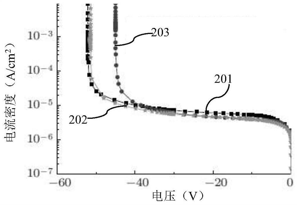
The invention discloses a TMBS device, which comprises a plurality of trench gate structures formed in an N-type epitaxial layer; a gate dielectric layer of each trench gate structure is divided intotwo parts; the dielectric constant of a material of a second gate dielectric layer of the top part of the side surface of each groove is greater than that of silicon dioxide of a first gate dielectriclayer at the bottom of the side surface of the groove; the depths of the side surfaces of the grooves covered with the second gate dielectric layers are greater than or equal to the junction depth ofschottky metal contact for reducing the electric field intensity of schottky metal contact areas, thereby reducing reverse leakage current of the TMBS device; and the N-type epitaxial layer at the bottoms of the schottky metal contact areas is covered with the side surfaces of the first gate dielectric layers to have relatively good electric field intensity distribution, thereby eliminating the influences of the second gate dielectric layers on reverse breakdown voltage of the device. The invention further discloses a manufacturing method of the TMBS device. According to the TMBS device, thereverse breakdown voltage and forward break-over voltage of the device can be kept when the reverse leakage current of the device is reduced.

Description

technical field [0001] The invention relates to the field of semiconductor integrated circuit manufacturing, in particular to a trench type MOS barrier Schottky diode (Trench MOS Barrier Controlled Schottky Rectifier, TMBS) device; the invention also relates to a manufacturing method of the TMBS device. Background technique [0002] Compared with the planar Schottky diode, the TMBS device adds a trench gate MOSFET structure. The surface between the trenches of the trench gate MOSFET forms a Schottky contact. The trench gate MOSFET is used in the reverse direction of the Schottky diode. The N-type epitaxial layer between the trenches is laterally depleted during biasing, which can increase the reverse breakdown voltage, which can also use a higher doping concentration or thinner N-type epitaxial layer, thereby reducing the device's Forward conduction resistance and forward conduction voltage (VF). [0003] Such as figure 1 As shown, it is a schematic structural view of an e...

Claims


Application Information

Patent Timeline
Patent Type & Authority Patents(China)
IPC IPC(8): H01L29/872H01L21/329
CPCH01L29/66143H01L29/8725
Inventor 石磊
Owner SHANGHAI HUAHONG GRACE SEMICON MFG CORP
Learn More