Optically pumped resonance enhanced flip-chip red LED device and preparation method thereof

A technology of LED devices and LED chips, which is applied in the direction of semiconductor devices, electrical components, circuits, etc., can solve the problems of complex red LED flip chip preparation process, difficulty in obtaining, high yield rate, etc., to avoid chip preparation process and cost The effect of low and high yield

Active Publication Date: 2019-11-29
INST OF SEMICONDUCTORS - CHINESE ACAD OF SCI
View PDF3 Cites 0 Cited by
  • Summary
  • Abstract
  • Description
  • Claims
  • Application Information

AI Technical Summary

Problems solved by technology

[0004] Unlike GaN-based blue-green flip-chip LEDs, the manufacturing process of AlGaInP-based red LED flip-chips is very complicated and it is difficult to obtain a high yield rate

Method used


Image

  • Optically pumped resonance enhanced flip-chip red LED device and preparation method thereof
  • Optically pumped resonance enhanced flip-chip red LED device and preparation method thereof

Examples


Embodiment Construction

[0033] In order to make the object, technical solution and advantages of the present invention clearer, the present invention will be described in further detail below in conjunction with specific embodiments and with reference to the accompanying drawings.

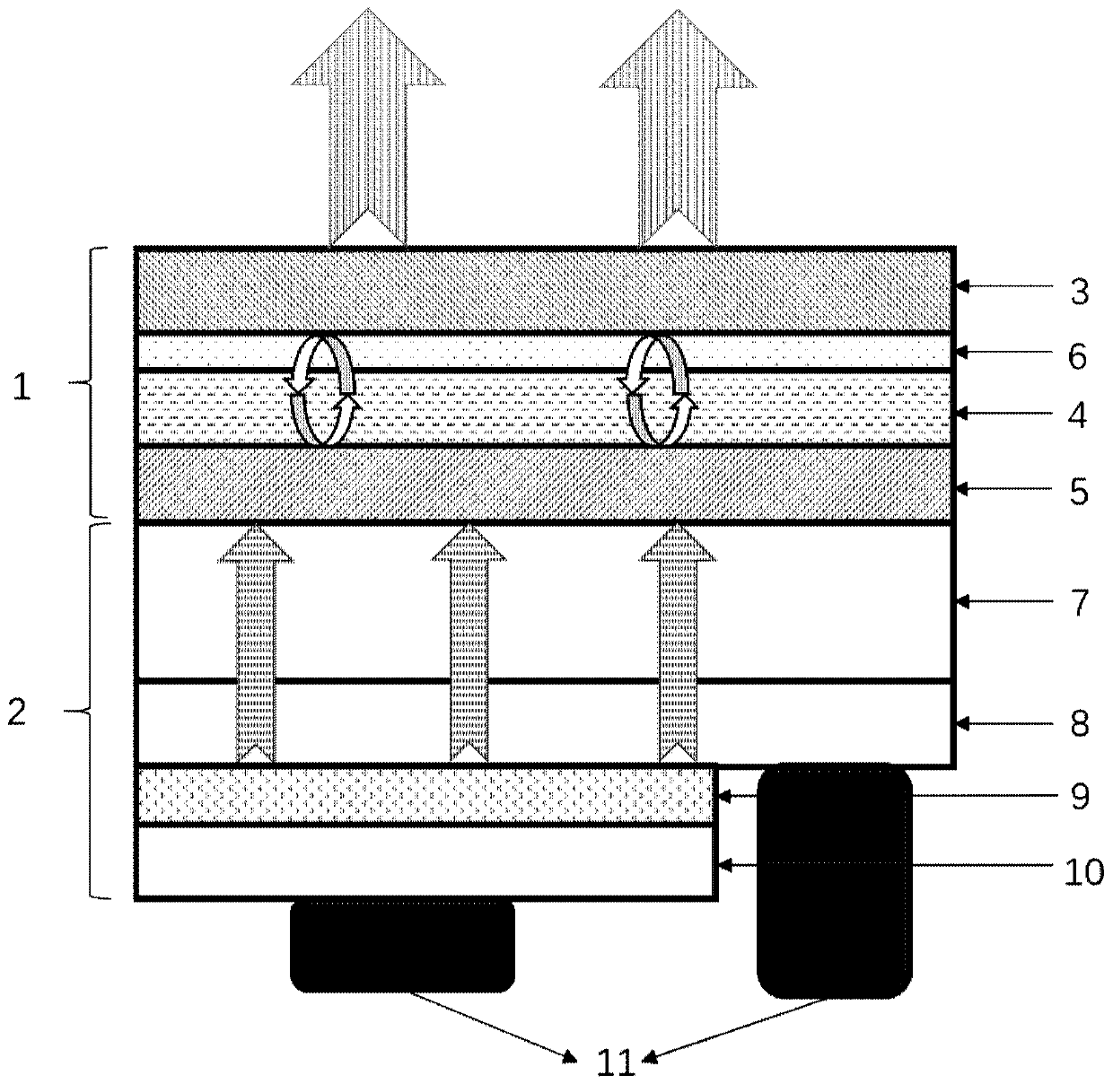
[0034] Such as figure 1 as shown, figure 1 It is a schematic structural diagram of an optically pumped resonance-enhanced flip-chip red LED device according to an embodiment of the present invention. The optically pumped resonance-enhanced flip-chip red LED device includes: a red LED quantum well structure 1 with a resonant cavity; A flip-chip blue LED chip 2 that fits on the incident surface of the red LED quantum well structure 1; wherein, the blue light photons emitted by the flip-chip blue LED chip 2 excite the red LED quantum well structure 1, so that the red LED quantum well Structure 1 emits red photons.

[0035] figure 1 Among them, the red LED quantum well structure 1 includes: the bottom Ta 2 o 5 / SiO 2 Br...


PUM


Abstract

The invention discloses an optical pump resonant enhanced inverted infrared LED device and a fabrication method thereof. The device comprises an infrared LED quantum-well structure and an inverted blue-light LED chip, wherein the infrared LED quantum-well structure is provided with a resonant cavity, an emergent surface of the inverted blue-light LED chip is bonded with an incident surface of theinfrared LED quantum-well structure, and the infrared LED quantum-well structure is simulated by blue-light photons emitted from the inverted blue-light LED chip so that the infrared LED quantum-wellstructure emits out red-light photons. In the device, the inverted red-light LED device absorbs photons emitted from the blue-light LED chip to give out light by an optical pump rather than traditional electrical injection light emitting, a traditional inverted red-light LED complicated epitaxial growth process and a chip fabrication process are prevented, the process complexity is reduced, the device reliability is improved, and the chip manufacturing process is shortened.

Description

technical field [0001] The invention relates to the technical field of optoelectronic devices, in particular to an optical pump resonance enhanced flip-chip red LED device and a preparation method thereof. Background technique [0002] Since the advent of red LED, it has been more than 40 years of development. Most of the red LEDs currently on the market are obtained by using MOCVD to epitaxially grow AlGaInP quaternary system materials on GaAs substrates. The internal quantum efficiency of red LED has reached more than 90%, and its material growth technology is quite mature. [0003] With the gradual rise of LED displays in recent years, the demand for RGB LEDs in the market has also increased rapidly, especially for small-sized LEDs. To achieve high-definition display of LED screens, the key technology is to reduce the luminous pixels of the display screen, that is, to reduce the chip size and arrangement spacing of RGB three-color LEDs; Or the eutectic welding process ...

Claims


Application Information

Patent Timeline
Patent Type & Authority Patents(China)
IPC IPC(8): H01L33/10H01L33/06H01L33/00
CPCH01L33/005H01L33/06H01L33/105
Inventor 王国宏陆兴东李璟李志聪
Owner INST OF SEMICONDUCTORS - CHINESE ACAD OF SCI
Why Eureka
Try Eureka