A method of making high precision mems inertial sensor using soi sheet

An inertial sensor, high-precision technology, applied in directions such as navigation through speed/acceleration measurement, can solve the problems of low precision of inertial sensors, low cross-axis sensitivity, etc., achieve low cross-sensitivity, low mechanical and thermal noise, and simplify the production process Effect

Active Publication Date: 2020-05-19
HUAZHONG UNIV OF SCI & TECH
View PDF2 Cites 0 Cited by
  • Summary
  • Abstract
  • Description
  • Claims
  • Application Information

AI Technical Summary

Problems solved by technology

[0006] For the above defects or improvement needs of the prior art, the object of the present invention is to provide a process method for making high-precision MEMS inertial sensors using SOI sheets, wherein through the selection of its key device layer and support layer and the variable-area periodic array type The configuration method of the capacitive displacement sensor is improved. Compared with the existing technology, it can effectively produce a large proof mass block and solve the problem of low precision of the MEMS inertial sensor. The out-of-plane direction movement can be realized by using the limit function of the SOI sheet support layer. protection, and can greatly simplify the packaging process; and, through the detailed structural design of the spring mass system, the present invention can effectively control their eigenfrequency, reduce mechanical and thermal noise, and achieve lower cross-axis sensitivity

Method used


Image

  • A method of making high precision mems inertial sensor using soi sheet
  • A method of making high precision mems inertial sensor using soi sheet
  • A method of making high precision mems inertial sensor using soi sheet

Examples


Embodiment 1

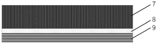
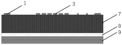
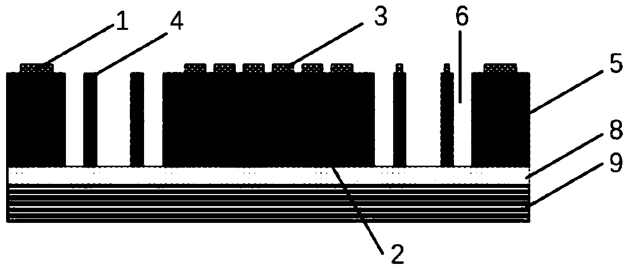
[0045] The material used is an SOI wafer, the thickness of the device layer 7 is 500 μm, the thickness of the sacrificial layer 8 is 1 μm, and the thickness of the supporting layer 9 is 100 μm. The device layer 7 can be a silicon layer, and the sacrificial layer 8 can be SiO 2 layer, the supporting layer 9 may be a silicon layer.

[0046] The realization technique of a kind of high-precision MEMS inertial sensor provided by the present invention comprises the following steps:

[0047] (1) complete the making of metal capacitor pole plate 3 and package contact point 1 on SOI silicon chip device layer 7, as Figure 2a shown. Further include the following steps:

[0048] (1-1) Carry out organic cleaning and oxygen plasma cleaning to the silicon wafer;

[0049] (1-2) Electron beam evaporation is used to plate titanium 40nm and gold 200nm on the surface of the silicon wafer (both refer to the thickness);

[0050] (1-3) performing photolithography on the surface of the metal la...

Embodiment 2

[0075] The material used is an SOI wafer, the thickness of the device layer 7 is 400 μm, the thickness of the sacrificial layer 8 is 2 μm, and the thickness of the supporting layer 9 is 50 μm.

[0076] The realization technique of a kind of high-precision MEMS inertial sensor provided by the present invention comprises the following steps:

[0077] (1) On the device layer 7 of the SOI silicon wafer, the fabrication of the metal capacitor plate 3 and the packaging contact point 1 is completed. Further include the following steps:

[0078] (1-1) Carry out organic cleaning and oxygen plasma cleaning to the silicon wafer;

[0079] (1-2) Evenly apply double-layer glue on the surface of the silicon wafer, after exposure and development, rinse with flowing deionized water for 5 minutes;

[0080] (1-3) Surface treatment of the sample, such as oxygen plasma cleaning, to ensure the cleanliness of the sample surface;

[0081] (1-4) Electron beam evaporation is used to plate titanium 40n...


PUM


Abstract

The invention discloses a method for utilizing an SOI sheet to manufacture a high-precision MEMS inertial sensor. The method mainly comprises the following steps that (1), the SOI sheet is treated, specifically, a driving plate capacitor and a packaging salient point are manufactured on a device layer of the SOI sheet, a silicon deep etching technology is adopted to process an etching trench to asacrificial layer of the SOI sheet, and integrated processing of a silicon base quality inspection block and a spring is completed; a mask is manufactured on a supporting layer, and the silicon deep etching technology is adopted to manufacture a releasing hole structure to the sacrificial layer of the SOI sheet; and the sacrificial layer of the SOI sheet is etched through the releasing holes, andthus movable parts are released; (2), a cover plate is manufactured; and (3), the SOI sheet and the cover plate are subjected to aligning packaging, and the MEMS inertial sensor is formed. By selecting the key device layer and the supporting layer, and improving a capacitor displacement detection mode, compared with the prior art, the method has the advantages that large quality inspection blockscan be manufactured effectively, a high capacitor displacement detection accuracy can be achieved, and the problem that the MEMS inertial sensor is low in accuracy is solved.

Description

technical field [0001] The invention belongs to the field of processing and manufacturing of microelectronic devices, and more specifically relates to a method for manufacturing a high-precision MEMS inertial sensor by using an SOI sheet. Background technique [0002] With the continuous development of micro-electromechanical systems (MEMS) technology and the maturity of silicon micro-machining technology, silicon micro-mechanical sensors are widely used in different fields due to their low price, high precision and suitability for mass production, such as automotive Various aspects of airbags, robot production and automation control. However, the accuracy of MEMS inertial sensors is low. Consumer electronics MEMS inertial sensors mostly use silicon surface technology. Due to the small thickness of the device layer, the proof mass is small and cannot achieve low mechanical and thermal noise. Industrial grade and MEMS inertial sensors for high-end applications mostly use SOI...

Claims


Application Information

Patent Timeline
Patent Type & Authority Patents(China)
IPC IPC(8): G01C21/16
CPCG01C21/16
Inventor 刘骅锋涂良成宋萧萧渠自强伍文杰
Owner HUAZHONG UNIV OF SCI & TECH
Why Eureka
Try Eureka