Preparation method of spectrum selective ITO thin film for automotive glass
An automotive glass, selective technology, applied in ion implantation plating, metal material coating process, coating, etc., can solve the problem of low reflectivity in the infrared region, achieve good visibility, increase transmittance, and increase reflectivity Effect
- Summary
- Abstract
- Description
- Claims
- Application Information
AI Technical Summary
Problems solved by technology
Method used
Image
Examples
Embodiment 1
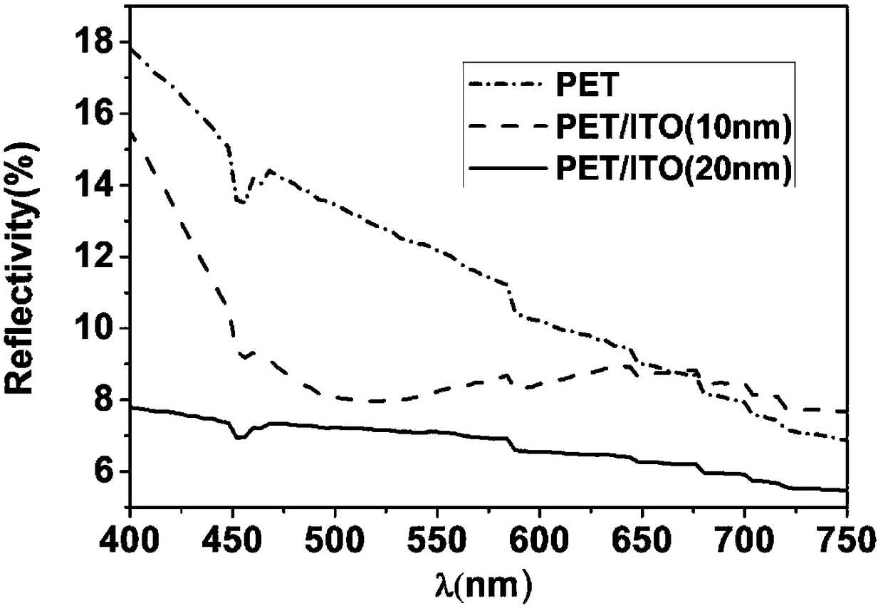
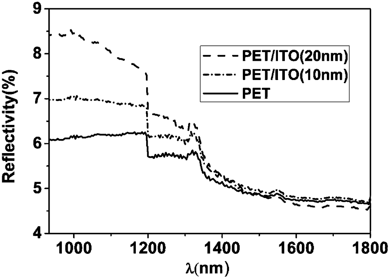
[0028] A preparation method for a spectrally selective ITO film for automotive glass, comprising the following steps:
[0029] (1) Clean the PET substrate, clean the surface and back of the PET substrate, and remove dust particles, organic and inorganic impurities;
[0030] a) strong ultrasonic cleaning in acetone solution for 3-5 minutes, and rinse with deionized water;
[0031] b) Strong ultrasonic cleaning in ethanol solution for 3-5 minutes, rinse with deionized water, high-purity N 2 Blow dry the surface and back;
[0032] c) Dry the water vapor in an oven at 120°C for about 20 minutes.
[0033] (2) Preparation before preparation of spectrally selective ITO thin film:
[0034] a) Install the ITO sputtering target, the purity of the ITO target is more than 99.999% atomic percent, the diameter of the ITO target is 50.8mm, and the background vacuum is 1×10 -4 Pa;
[0035] b) Set the sputtering power to 30W;
[0036] c) Using high-purity Ar gas as the sputtering gas (vo...
Embodiment 2
[0041] The preparation method of the ITO thin film among the present embodiment and embodiment 1 is basically the same, and the difference is: in (3) b), the sputtering time is 1040s, and the ITO thin film thickness that finally obtains is 20nm namely conductive thin film PET / ITO ( 20nm).
Embodiment 3
[0043] The preparation method of the ITO thin film among the present embodiment and embodiment 1 is basically the same, and difference is: sputtering power is 25W, and the gas flow rate of Ar gas is 25sccm, and sputtering air pressure is 0.35Pa; In (3) b), The sputtering time is 780s, and the thickness of the finally obtained ITO film is 12nm, that is, the conductive film PET / ITO (12nm).
PUM
| Property | Measurement | Unit |
|---|---|---|
| thickness | aaaaa | aaaaa |
| thickness | aaaaa | aaaaa |
| thickness | aaaaa | aaaaa |
Abstract
Description
Claims
Application Information
 - R&D
- Intellectual Property
- Life Sciences
- Materials
- Tech Scout
- Unparalleled Data Quality
- Higher Quality Content
- 60% Fewer Hallucinations
Browse by: Latest US Patents, China's latest patents, Technical Efficacy Thesaurus, Application Domain, Technology Topic, Popular Technical Reports.
© 2025 PatSnap. All rights reserved.Legal|Privacy policy|Modern Slavery Act Transparency Statement|Sitemap|About US| Contact US: help@patsnap.com


