Laser cleaning process
A laser cleaning and process technology, applied in the field of laser processing, can solve problems such as low production capacity, high metal loss, and failure of phosphating layer, and achieve the effects of stable and reliable quality, high processing efficiency, and reduced impact
- Summary
- Abstract
- Description
- Claims
- Application Information
AI Technical Summary
Problems solved by technology
Method used
Image
Examples
Embodiment 1
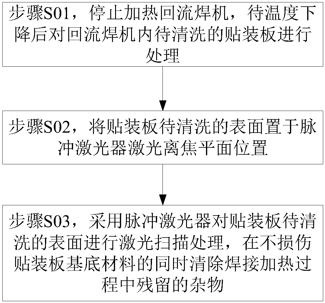
[0023] The laser cleaning process of the present embodiment comprises the following specific steps:
[0024] Step S01: Stop heating the reflow soldering machine in working state, open the outer cover after the temperature drops to 40°C, and check the residual solder balls and solder resist on the surface of the internal mounting board;
[0025] Step S02: Using a pulsed laser with a laser wavelength of 1064nm, place the surface of the mounting board to be cleaned on the laser out-of-focus plane. The surface of the mounting board to be cleaned is solder balls, solder resist, etc. remaining during the welding heating process Debris, especially the position on the surface of the clogged pores; the position of the laser from the focal plane is positive defocus 20mm, located above the focal plane, so that the power density distribution of the laser spot is relatively uniform, and when processing the surface of the mounting board, if the laser energy is too large Concentrated, it is ...
Embodiment 2
[0028] A kind of laser cleaning process of the present embodiment comprises the following specific steps:
[0029] Step S01: Stop heating the reflow soldering machine in working state, open the outer cover after 50°C, and check the residual solder balls and solder resist on the surface of the internal mounting board;
[0030] Step S02: Using a pulsed laser with a laser wavelength of 1064nm, using laser processing technology, place the surface of the mounting board to be cleaned on the laser defocus plane for scanning; the surface of the mounting board to be cleaned is the residual Solder balls, solder resist and other sundries, especially the position on the surface of the clogged pores; the defocus plane position of the laser is negative defocus 20mm, which is located below the focal plane, so that the power density distribution of the laser spot is relatively uniform, and when processing the mounting board On the surface, if the laser energy is too concentrated, it is easy t...
PUM
| Property | Measurement | Unit |
|---|---|---|
| wavelength | aaaaa | aaaaa |
| wavelength | aaaaa | aaaaa |
Abstract
Description
Claims
Application Information
