High-luminance LED chip and manufacturing method thereof

A technology of LED chips and manufacturing methods, applied in electrical components, circuits, semiconductor devices, etc., can solve the problem that LED chips cannot fully meet the needs of people's lives, improve luminous efficiency and reliability, facilitate the passage of current, and reduce absorption. Effect

Inactive Publication Date: 2018-06-29
XIANGNENG HUALEI OPTOELECTRONICS
View PDF9 Cites 9 Cited by
  • Summary
  • Abstract
  • Description
  • Claims
  • Application Information

AI Technical Summary

Problems solved by technology

However, the above-mentioned LED chips still cannot fully meet people's living needs.

Method used


Image

  • High-luminance LED chip and manufacturing method thereof
  • High-luminance LED chip and manufacturing method thereof
  • High-luminance LED chip and manufacturing method thereof

Examples


Embodiment Construction

[0041] The embodiments of the present invention will be described in detail below with reference to the accompanying drawings, but the present invention can be implemented in various ways defined and covered by the claims.

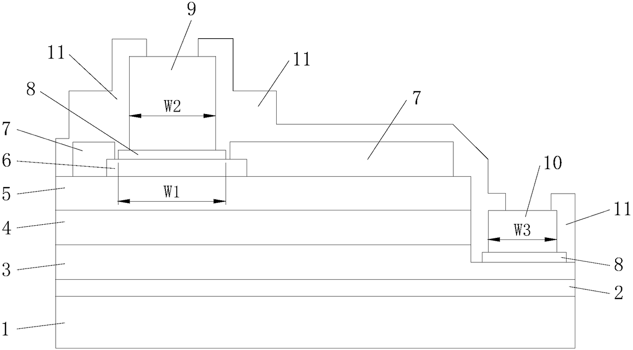
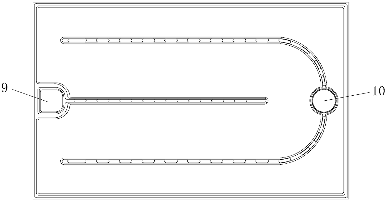
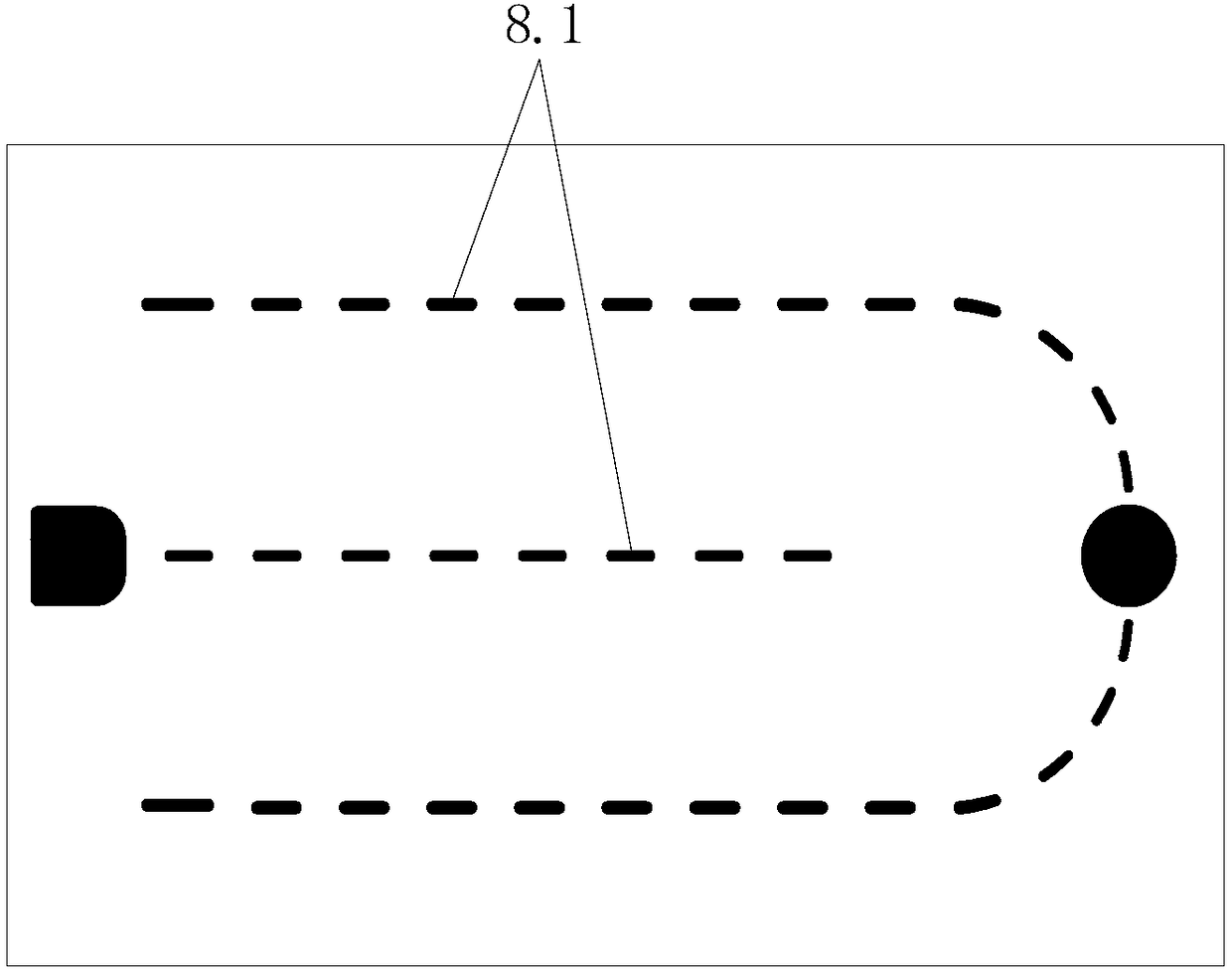
[0042] see Figure 1 to Figure 3 , a high-brightness LED chip of the present invention, comprising:

[0043] The epitaxial wafer includes a substrate material 1 and a buffer layer 2 , an N-type semiconductor layer 3 , a light-emitting layer 4 and a P-type semiconductor layer 5 sequentially formed on the substrate material 1 . Wherein, the substrate material 1 may be one of Si substrate material, sapphire substrate material, SiC substrate material and other materials. The epitaxial wafer has a stepped structure including an upper stepped surface and a lower stepped surface. The upper stepped surface is a P-type semiconductor layer 5, and the lower stepped surface is an N-type semiconductor layer 3. The connection between the upper stepped surface and the low...


PUM


Abstract

The invention discloses a high-luminance LED chip and a manufacturing method thereof. The high-luminance LED chip comprises an epitaxial wafer, a current barrier layer, a current expanding layer, reflecting layers, a P electrode, an N electrode and a transparent insulation layer, wherein the epitaxial wafer comprises a substrate material, a buffer layer, an N-type semiconductor layer, a luminancelayer and a P-type semiconductor layer, the N-type semiconductor layer, the luminance layer and the P-type semiconductor layer are formed on the substrate material in sequence, the current barrier layer is formed on the P-type semiconductor layer, the current expanding layer is formed on the P-type semiconductor layer, the reflecting layers are formed in the current barrier layer and a lower stepface and comprise multiple reflecting layer subsections which are arranged at equal intervals, the P electrode is formed on the reflecting layer on the current barrier layer, and the N electrode is formed on the reflecting layer on the lower step face. By means of the high-luminance LED chip and the manufacturing method thereof, the reflecting layers are arranged below the electrodes, the absorption of light by the electrodes can be further reduced, the reflecting efficiency to light by the electrodes is improved, and the luminance of the LED chip is further improved; meanwhile, the arrangement of the reflecting layers is beneficial to improving of the current distribution efficiency, and thus the luminous efficiency and reliability of the LED chip are improved.

Description

technical field [0001] The invention relates to the technical field of semiconductor chips, in particular to a high-brightness LED chip and a manufacturing method thereof. Background technique [0002] At present, the third-generation semiconductor materials have been widely used in various fields of human production and life, and play an important role in them. Gallium nitride (GaN) material, as an important part of the third-generation semiconductor material family, has also been widely used, and it plays an irreplaceable role in the LED semiconductor industry. GaN material is a hexagonal wurtzite structure, which has the advantages of stable chemical properties, high temperature resistance, large band gap, and high electron drift saturation velocity. Therefore, GaN-based materials are widely used in the preparation of electronic devices such as LED chips, blue LEDs, green LEDs, and ultraviolet LEDs, and are widely used in various fields of production and life such as lig...

Claims


Application Information

Patent Timeline
Patent Type & Authority Applications(China)
IPC IPC(8): H01L33/46H01L33/14H01L33/40
CPCH01L33/46H01L33/145H01L33/405H01L2933/0016
Inventor 周智斌李峰廖小花吴慧娟
Owner XIANGNENG HUALEI OPTOELECTRONICS
Why Eureka
Try Eureka