Preparation method of twenty-six-side CsPbX3 perovskite nanocrystalline

A technology of hexahedron and perovskite, applied in nanotechnology, nanotechnology, nanotechnology, etc. for materials and surface science, can solve the unfavorable growth process of perovskite nanocrystals, uneven morphology, etc. problems, to achieve the effects of controllable components, easy adjustment of product size, and simple operation

Inactive Publication Date: 2018-07-03
JILIN UNIV
View PDF4 Cites 8 Cited by
  • Summary
  • Abstract
  • Description
  • Claims
  • Application Information

AI Technical Summary

Problems solved by technology

However, due to the presence of excess precursors and ligands such as oleylamine and oleic acid in the synthesis process, the morphology and size of the prepared nanocrystals have a certain size distribution, and the morphology is not uniform, which is not conducive to understanding pure inorganic CsPbX 3 Growth process of perovskite nanocrystals

Method used


Image

  • Preparation method of twenty-six-side CsPbX3 perovskite nanocrystalline
  • Preparation method of twenty-six-side CsPbX3 perovskite nanocrystalline
  • Preparation method of twenty-six-side CsPbX3 perovskite nanocrystalline

Examples


Embodiment 1

[0028] First, a cesium oleate solution is prepared. Take 2mmol (0.648g) of cesium carbonate powder, 10mmol (3.35mL) of OA (oleic acid) and 6.65mL of ODE (octadecene) and mix them, heat to 150°C under nitrogen protection to dissolve cesium carbonate, cool to 100 ℃, prepared into 0.2M cesium oleate solution, which was light yellow transparent solution.

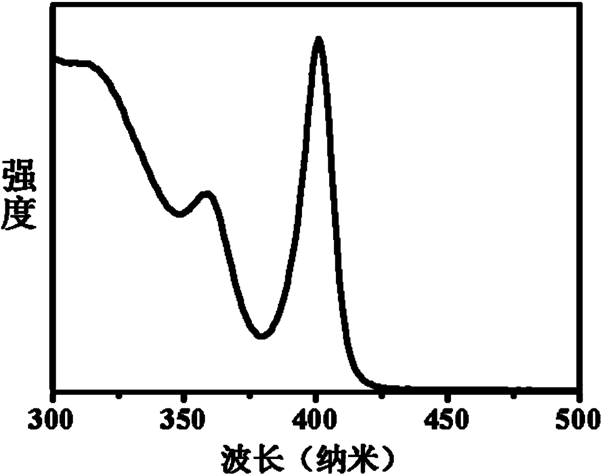
[0029] Then take 0.2mmol of lead bromide solid powder, 0.6mL of oleylamine, 0.6mL of oleic acid and 2.8mL of octadecene into the three-necked flask, vacuumize at 50°C for 30 minutes, fill with nitrogen protection, and then heat up to 150°C , after the lead bromide is dissolved, lower it to room temperature 25°C, and then inject 0.2mL of 0.2M cesium oleate octadecene solution, and react to obtain CsPbBr with an absorption peak at 402nm 3 Perovskite nanocrystalline seeds. Its absorption spectrum is shown in figure 1 .

Embodiment 2

[0031] The 0.04mmol of CsPbBr prepared in Example 1 3 The perovskite nanocrystal seeds were centrifuged, precipitated and dispersed into 4 mL of octadecene.

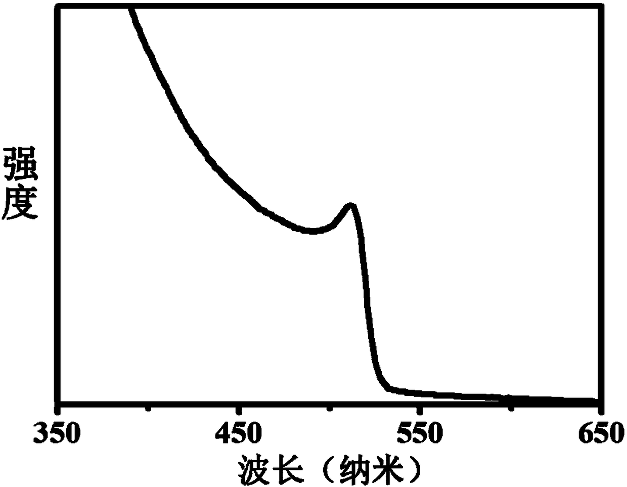
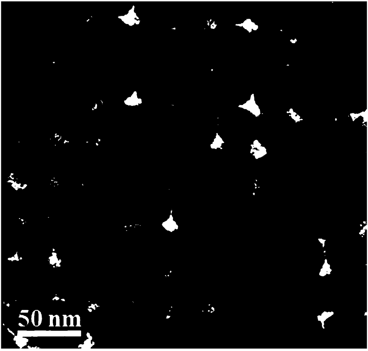
[0032] Take the above 4mL CsPbBr 3The octadecene solution of perovskite nanocrystal seeds was added to a three-neck flask, filled with nitrogen for protection, added 0.02 mmol of stearyl phosphoric acid, and then heated to 205 ° C, and the reaction obtained CsPbBr with an absorption peak at 512 nm 3 Perovskite nanocrystals with a particle size of 28nm. Its absorption spectrum is shown in Figure 4 , see its electron micrograph Figure 5 .

Embodiment 3

[0034] The 0.04mmol of CsPbBr prepared in Example 1 3 The perovskite nanocrystal seeds were centrifuged, precipitated and dispersed into 4 mL of octadecene.

[0035] Take the above 4mL CsPbBr 3 The octadecene solution of the perovskite nanocrystal seeds was added to the three-neck flask, filled with nitrogen for protection, added 0.02 mmol of octadecyl phosphoric acid, and then heated to 215 ° C, and the reaction obtained CsPbBr with an absorption peak at 514 nm 3 Perovskite nanocrystals with a particle size of 36nm. Its absorption spectrum is shown in Figure 6 , see its electron micrograph Figure 7 .


PUM

PropertyMeasurementUnit
sizeaaaaaaaaaa
sizeaaaaaaaaaa
sizeaaaaaaaaaa

Abstract

The invention discloses a preparation method of twenty-six-side CsPbX3 perovskite nanocrystalline, belonging to the technical field of semiconductor nano materials. The preparation method comprises the following steps: firstly, adding a carboxylic acid caesium solution into a lead bromide solution protected by N2, and carrying out reaction to obtain CsPbBr3 perovskite nanocrystalline seeds; then dispersing CsPbBr3 perovskite nanocrystalline seeds into octadecylene, adding octadecyl phosphoric acid, raising the temperature to preset temperature, and carrying out reaction to obtain CsPbBr3 perovskite nanocrystallines with different sizes and twenty-six sides in morphology, and finally, dispersing the CsPbBr3 perovskite nanocrystallines into normal hexane, and dropwise adding a lead chloridesolution or lead iodide solution, and carrying out reaction to obtain CsPbX3 (X=Cl, I, Cl / Br or I / Br) perovskite nanocrystalline with other components and twenty-six sides in morphology. The preparation method has the advantages of simple operation, easily adjustable product size, controllable components and the like.

Description

technical field [0001] The invention belongs to the technical field of semiconductor nanomaterial preparation, and relates to a large-size hexahedron CsPbX 3 Preparation methods of perovskite nanocrystals. Background technique [0002] When the size of the particle reaches the nanometer level, the electronic energy level near the Fermi level splits into discrete energy levels from a continuous state. For semiconductor materials reduced to nanometer size, it is especially smaller than or equal to the excitonic Bohr radius of the material. , the nearly continuous energy bands are now transformed into discrete energy levels. Quantum dots refer to semiconductor nanocrystals with a quantum confinement effect usually between 1 and 100 nm in size. The more common quantum dots mainly include II-VI and III-V semiconductors. They have excellent optical and photoelectric properties, such as broad absorption spectrum, narrow emission spectrum, high luminous efficiency, anti-photoblea...

Claims


Application Information

Patent Timeline
Patent Type & Authority Applications(China)
IPC IPC(8): C01G21/00B82Y30/00B82Y40/00
CPCB82Y30/00B82Y40/00C01G21/006C01P2002/34C01P2004/64
Inventor 张颖刘峰解仁国汪大洋杨文胜
Owner JILIN UNIV
Why Eureka
Try Eureka