Light-emitting diode epitaxial wafer and manufacture method thereof

A technology of light-emitting diodes and manufacturing methods, which is applied in the direction of electrical components, circuits, semiconductor devices, etc., can solve the problems of low quantum efficiency in LEDs, damage to multiple quantum well layers, etc., to improve growth temperature, increase hole concentration, The effect of improving the activation ability

Active Publication Date: 2018-07-13
HC SEMITEK SUZHOU
View PDF3 Cites 2 Cited by
  • Summary
  • Abstract
  • Description
  • Claims
  • Application Information

AI Technical Summary

Problems solved by technology

[0006] In order to solve the problem in the prior art that the high content of Al in the electron blocking layer causes low internal quantum efficiency of the LED, and the growth of the electron blocking layer at high temperature will destroy the multi-quantum well layer, the embodiment of the present invention provides a light emitting diode Epitaxial wafer and its manufacturing method

Method used


Image

  • Light-emitting diode epitaxial wafer and manufacture method thereof
  • Light-emitting diode epitaxial wafer and manufacture method thereof

Examples


Embodiment 1

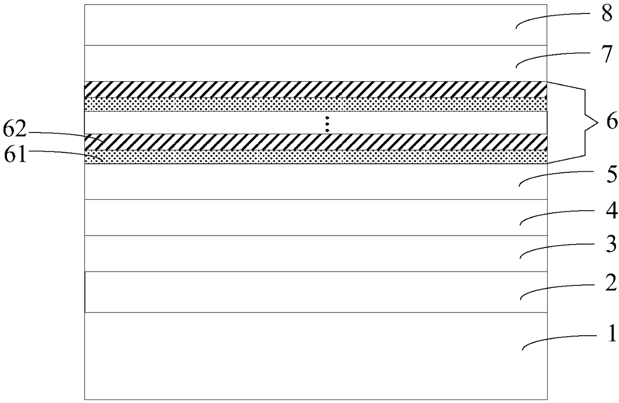
[0031] An embodiment of the present invention provides a light emitting diode epitaxial wafer, figure 1 It is a schematic structural diagram of a light-emitting diode epitaxial wafer provided by an embodiment of the present invention, as shown in figure 1 As shown, the gallium nitride-based light-emitting diode includes a substrate 1, a buffer layer 2, an undoped GaN layer 3, an N-type layer 4, a multi-quantum well layer 5, and an electron blocking layer stacked on the substrate 1 in sequence. 6. High temperature P-type layer 7 and P-type contact layer 8 .

[0032] Wherein, the electron blocking layer 6 is a superlattice structure including N periods, and the superlattice structure of each period includes In near the multi-quantum well layer. x Ga 1-x N layer 61 and Al away from multiquantum well layer 5 y Ga 1-y N layer 62, 0.1≤x≤0.2, 0≤y≤0.2, In x Ga 1-x The In content in the N layer 61 is less than the In content in the multi-quantum well layer 5, and the Al y Ga 1-...

Embodiment 2

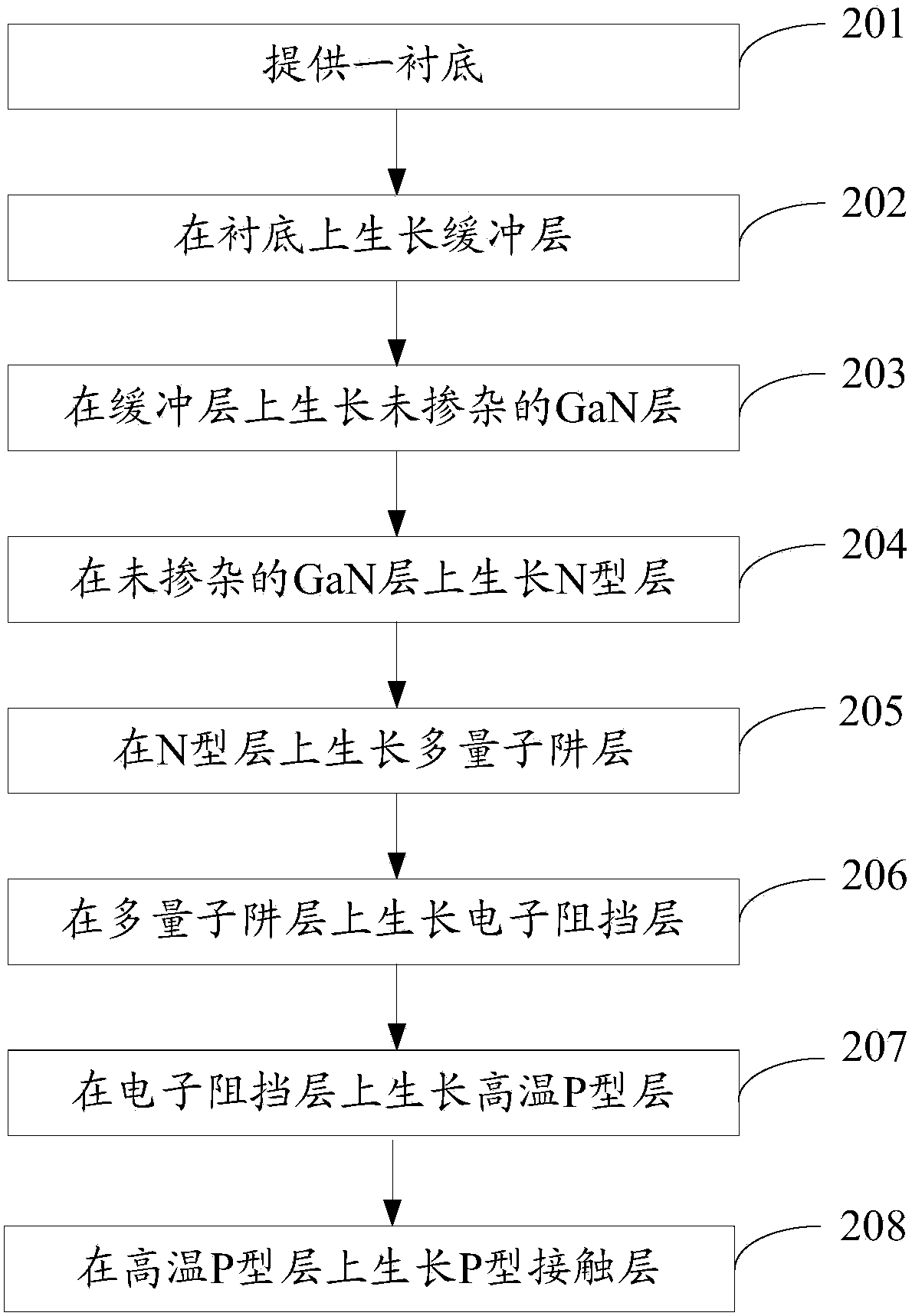
[0052] An embodiment of the present invention provides a method for manufacturing a light-emitting diode epitaxial wafer, which is suitable for the light-emitting diode epitaxial wafer provided in Embodiment 1. figure 2 It is a flow chart of a method for manufacturing a light-emitting diode epitaxial wafer provided by an embodiment of the present invention, as shown in figure 2 As shown, the manufacturing method includes:

[0053] Step 201, providing a substrate.

[0054] Specifically, the substrate is sapphire with a thickness of 630-650 μm.

[0055] In this embodiment, Veeco K465i or C4MOCVD (Metal Organic Chemical VaporDeposition, metal organic compound chemical vapor deposition) equipment is used to realize the LED growth method. Using high-purity H 2 (hydrogen) or high-purity N 2 (nitrogen) or high purity H 2 and high purity N 2 The mixed gas as the carrier gas, high-purity NH 3 As N source, trimethylgallium (TMGa) and triethylgallium (TEGa) as gallium source, trim...


PUM


Abstract

The invention discloses a light-emitting diode epitaxial wafer and a manufacture method thereof and belongs to the technical field of semiconductors. The light-emitting diode epitaxial wafer comprisesan electronic barrier layer that includes superlattice structure of N cycles; the superlattice structure of each cycle includes an InxGa1-xN layer and an AlyG1-yN layer, wherein the InxGa1-xN layer is formed by growth at 900-950 DEG C; lattice quality of a multi-quantum well layer can be improved, composite light-emitting efficiency of electrons and holes in the multi-quantum well layer can be improved. In addition, the presence of In brings down activation energy of Mg and increases hole concentration of a P-type layer. Each AlyG1-yN layer is formed by growth at 950-980 DEG C, barrier heightof the AlyG1-yN layer is increased, and electrons are avoided overflowing to the P-type layer; the content of Al gradually decreases or increases, so that electrons can be avoided overflowing to theP-type layer at the premise of reducing the blocking action of holes, and light-emitting efficiency of a diode is improved.

Description

technical field [0001] The invention relates to the technical field of semiconductors, in particular to a light-emitting diode epitaxial wafer and a manufacturing method thereof. Background technique [0002] LED (Light Emitting Diode, Light Emitting Diode) is a semiconductor electronic component that can emit light. As an efficient, environmentally friendly and green new solid-state lighting source, GaN-based LED devices are being rapidly and widely used, such as traffic lights, outdoor full-color display screens, urban landscape lighting, automotive interior and exterior lights, mobile phone backlights Wait. [0003] GaN-based LED epitaxial wafer is the main structure of GaN-based LED devices. The structure of GaN-based LED epitaxial wafer includes: substrate, buffer layer stacked on the substrate, undoped GaN layer, N-type layer, multi-quantum Well layer, high temperature P-type layer and P-type contact layer. The main reason for the low luminous efficiency of GaN-base...

Claims


Application Information

Patent Timeline
Patent Type & Authority Applications(China)
IPC IPC(8): H01L33/04H01L33/06H01L33/14H01L33/00
CPCH01L33/007H01L33/04H01L33/06H01L33/145
Inventor 蒋媛媛李昱桦胡加辉
Owner HC SEMITEK SUZHOU
Why Eureka
Try Eureka