OLED luminous composition and preparation method thereof
A composition and compound technology, applied in the direction of luminescent materials, chemical instruments and methods, semiconductor/solid-state device manufacturing, etc., to achieve the effect of excellent photoelectric performance
- Summary
- Abstract
- Description
- Claims
- Application Information
AI Technical Summary
Problems solved by technology
Method used
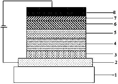
Image

Examples
Embodiment 1
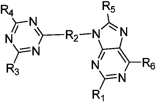
[0063] Taking Example 1 as an example, the synthetic route is as follows:
[0064]
[0065] Embodiment one:
[0066] Step 1) Preparation of Intermediate-1:
[0067] Throw in 40.0g (0.17mol) 4,6-dichloro-2-phenyl-5-aminopurine, 54.1g (0.17mol) 4,6-diphenyl-2-(4-aminophenyl)-1, 3,5-Triazine as the raw material, 1.926g (0.0017mol) tetrakistriphenylphosphorous palladium, 48.0g (0.5mol) sodium tert-butoxide, and 500.0g xylene, heated to 100-110°C, kept the temperature for 9hrs, Cool down to room temperature, add 300.0g of water, separate layers, desolventize the organic phase to obtain 98.3g of brown oily liquid, and obtain 18.6g (0.035mol) of Intermediate-1 by column chromatography;
[0068] Step 2) Preparation of Intermediate-2:
[0069] Add 18.6g (0.035mol) of intermediate-1 and 4.95g (0.035mol) of benzoyl chloride, 300.0g of DMF and 95.0g of silica gel loaded with ferric chloride (the content of aluminum chloride is 9%, about 0.053mol) , raised the temperature to 100-110...
PUM
 Abstract
Description
Claims
Application Information
 - R&D
- Intellectual Property
- Life Sciences
- Materials
- Tech Scout
- Unparalleled Data Quality
- Higher Quality Content
- 60% Fewer Hallucinations
Browse by: Latest US Patents, China's latest patents, Technical Efficacy Thesaurus, Application Domain, Technology Topic, Popular Technical Reports.
© 2025 PatSnap. All rights reserved.Legal|Privacy policy|Modern Slavery Act Transparency Statement|Sitemap|About US| Contact US: help@patsnap.com