

Preparation method of semiconductor film composite structural member
A composite structure, semiconductor technology, applied in the direction of semiconductor devices, electric solid devices, electrical components, etc., can solve the problems of easily damaged circuit structure, complicated circuit connection operation, affecting device performance, etc., to achieve easy control, ensure excellent performance, The effect of broad market prospects
- Summary
- Abstract
- Description
- Claims
- Application Information
AI Technical Summary
Problems solved by technology
Method used
Image

Examples
preparation example Construction
[0028] The invention provides a method for preparing a semiconductor thin film composite structure, comprising the following steps:
[0029] a) setting a pixel lattice structure and a readout circuit on the surface of the substrate, the pixel lattice structure is composed of a plurality of pixel units;
[0030] b) Place the substrate provided with the pixel lattice structure and the readout circuit in the wide-bandgap oxide film growth equipment; block the readout circuit with a mask, and carry out the wide-bandgap oxide film under the condition of 20-450°C The film layer is grown to obtain a semiconductor thin film composite structure.
[0031] In the preparation method provided by the present invention, firstly, a pixel lattice structure and a readout circuit are arranged on the surface of the substrate. Wherein, the substrate includes but is not limited to a sapphire substrate; the pixel lattice structure is composed of a plurality of pixel units, each of which is composed...
Embodiment 1
[0039] Prepare the semiconductor film-substrate composite structure, the specific steps are as follows:
[0040] 1) Make a 3×3 pixel lattice structure and a readout circuit on a sapphire substrate; wherein, each pixel unit in the pixel lattice structure is composed of two independent electrode units, and the electrode units are made of gold Composed of an interdigitated structure, the length of the interdigitated fingers is 0.5 mm, the finger width and interdigital spacing are 10 μm, and the number of interdigitated pairs is 50 pairs; the readout circuit is connected to each of the pixel units respectively (the readout circuit There are two contacts in the output circuit, and each contact is correspondingly connected to an electrode unit in the pixel unit), and the material used for the connection is a gold wire with a diameter of 25 μm;
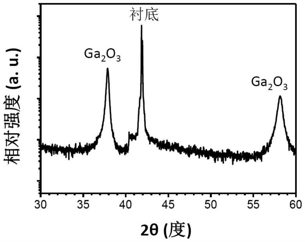
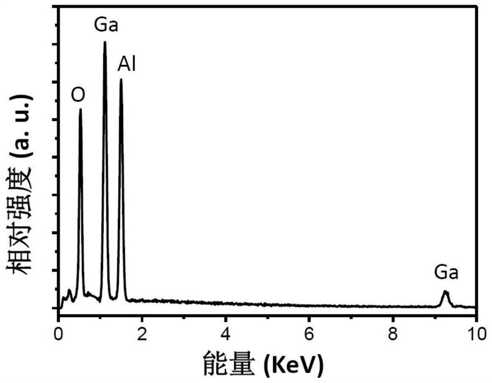
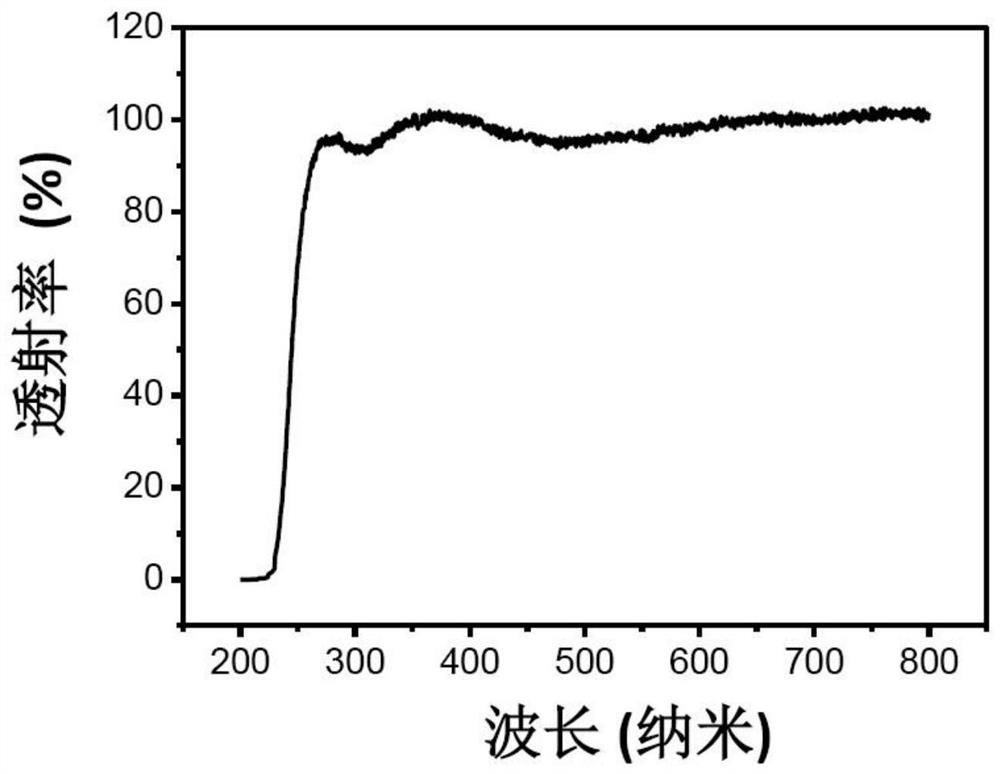
[0041] 2) Put the substrate material with the pixel lattice structure and readout circuit on the surface into the MOCVD growth equipment, b...
Embodiment 2
[0048] Referring to the preparation steps of Example 1, the only difference is that the Ga 2 o 3 The growth method of the film was replaced by magnetron sputtering by MOCVD. The specific magnetron sputtering conditions were: the sputtering RF power was 100W, and the sputtering pressure was 1×10 -1 Pa, the sputtering time is 2h; the substrate material that will complete the growth of the film layer is gradually cooled to room temperature, and the cooling method is preferably natural cooling.
[0049] The optoelectronic properties of the semiconductor thin film-substrate composite structure prepared in this example were tested by the readout circuit on the substrate. The specific method refers to Example 1. The results show that the photocurrent is 15 μA and the 90-10% response time is 480 ms.
PUM
| Property | Measurement | Unit |
|---|---|---|
| Thickness | aaaaa | aaaaa |
| Diameter | aaaaa | aaaaa |
| Diameter | aaaaa | aaaaa |
Abstract
Description
Claims
Application Information