High-sensitivity sensor with linear-induced cracks and manufacturing method thereof
A high-sensitivity, sensor technology, applied in the direction of sensors, instruments, force/torque/power measuring instruments, etc., to achieve high economic efficiency
- Summary
- Abstract
- Description
- Claims
- Application Information
AI Technical Summary
Problems solved by technology
Method used
Image

Examples
Embodiment 1
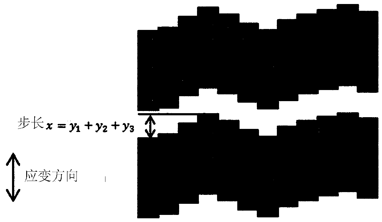
[0176] Fabrication of a high-sensitivity sensor based on an induction crack
[0177] like image 3 a ~ 3c shown in the manufacture of crack sensors.
[0178] Specifically, using a plasma surface treatment machine CUTE-1MPR (Femto Science Inc.), spin-coated 100 μm polydimethylsiloxane (PDMS) was treated with oxygen plasma and bonded on on the glass. After 20 μl of polyurethane acrylate (PUA) was dropped on the PDMS / glass mold, the filler-patterned silicone mold was covered and treated with 350nm UV (approximately 12mJ / cm 2 ) irradiation. Thermal evaporation was performed by a thermal evaporator (Selcos Inc.) to form a 10 nm patterned chromium layer and a sputtered 20 nm platinum layer was deposited. The PUA film deposited with the metal layer was carefully removed from the PDMA / glass mold and then stretched by 5% in the x / y direction using a custom-made stretcher. Figure 4 The crack sensor before and after stretching is shown in .
[0179] Then, a conductive polymer is ...
Embodiment 2
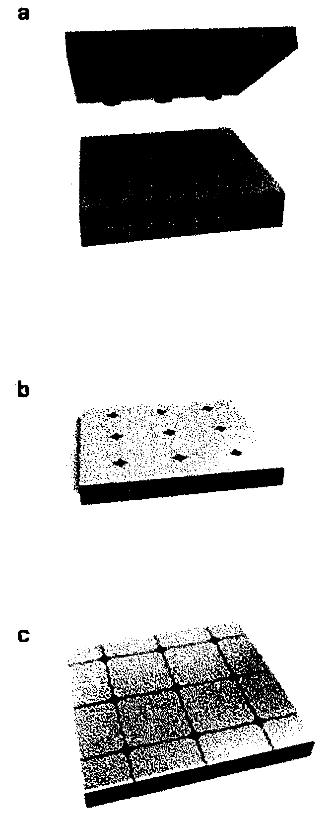
[0180] Manufacture of multi-pixel array sample
[0181] To demonstrate the scalability and capabilities of devices for detecting mechanical shock and pressure, such as Figure 16 As shown in b, in 6×6cm 2 A sensor network of 16 pixels (4×4 pixel array) is set on the area. Figure 16 a and Figure 16 a shows a schematic diagram of the multi-pixel system. Each pixel (1×1cm 2 Islands) consisted of 100 μm thick PUA / 10 nmCr / 20 nm Pt with a hole pattern, which was then bidirectionally elongated and stretched by 10% to create cracks. The electrical connection between the cracked Pt and the Lab View-based PXI-4071 system (NIinstrument Inc.) was formed by gold wires (Au, 50 nm thick) deposited on the PET film using the hatching method. Each fabricated pixel was placed on a PET film with electrical connections via a conductive polymer (CW2400, Circuit Engineering) or via gold wires in an independent manner.
experiment example 1
[0182] Measuring the change in resistance according to the length of the crack gap (measurement coefficient)
[0183] In order to confirm the effect of linear cracks using the high-sensitivity sensor of Example 1, cracks were formed by using three different hole patterns.
[0184] like Figure 7 In a, P is the shortest distance between the hole centers and is the same in all three test patterns, G is the length of the gap, and the gap represents the shortest distance between the tips of the holes.
[0185] When the length of G is 10μm, 15μm and 20μm, in Image 6 a and Image 6 b and Figure 7 The crack formation patterns and resistance changes are shown in a to 7d.
[0186] Image 6 a shows that when the length of the gap G is 10 μm and 15 μm, several cracks can be induced, while Image 6 b shows that when G is 20 μm, very straight cracks are produced. like Image 6 As shown in a, the presence of many incomplete cracks may reduce the sensitivity to resistance changes,...
PUM
 Abstract
Description
Claims
Application Information
 - Generate Ideas
- Intellectual Property
- Life Sciences
- Materials
- Tech Scout
- Unparalleled Data Quality
- Higher Quality Content
- 60% Fewer Hallucinations
Browse by: Latest US Patents, China's latest patents, Technical Efficacy Thesaurus, Application Domain, Technology Topic, Popular Technical Reports.
© 2025 PatSnap. All rights reserved.Legal|Privacy policy|Modern Slavery Act Transparency Statement|Sitemap|About US| Contact US: help@patsnap.com